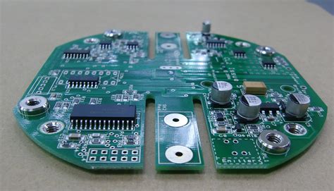
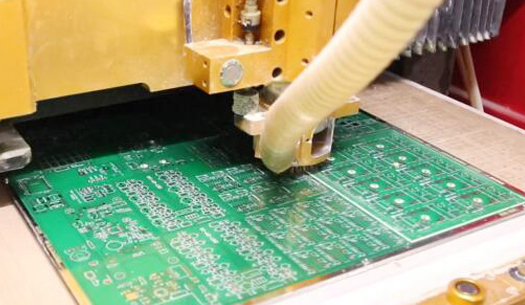
multilayer pcb design

1. What is a multilayer pcb
The biggest difference between a PCB multilayer board and a single-sided and double-sided board is the addition of an internal power layer and ground layer. The power and ground networks are mainly routed on the power layer.
There is conductive metal on both sides of each substrate layer on a PCB multilayer board, and a special adhesive is used to connect the boards together, and there is an insulating material between each board. However, PCB multilayer wiring is mainly based on the top and bottom layers, supplemented by an intermediate wiring layer.
The key is how to optimize the wiring of the internal electrical layer to make the wiring of the circuit board more reasonable. An inevitable product of multifunctional development, large capacity and small volume.
Therefore, the design of a multilayer PCB board is basically the same as the design method of a double-sided board.
With the continuous development of electronic technology, especially the extensive and in-depth application of large-scale and ultra-large-scale integrated circuits, multilayer PCBs are rapidly developing towards high density, high precision and high-level digitization. Fine lines, small aperture penetration and blind hole technologies such as buried holes and high board thickness aperture ratios can meet market demand.
PCB multilayer printed boards are widely used in the manufacture of electronic products due to their flexible design, stable and reliable electrical performance and excellent economic performance.
Especially with the extensive and in-depth application of large-scale and ultra-large-scale integrated circuits, multi-layer PCBs are developing towards high density, high precision and high level of digitalization.
Fine lines, small aperture penetration and blind hole technologies such as buried holes and high plate thickness aperture ratio can meet market demand.
PCB multi-layer printed boards are widely used in the manufacture of electronic products due to their flexible design, stable and reliable electrical performance and excellent economic performance. Especially with the extensive and in-depth application of large-scale and ultra-large-scale integrated circuits, multi-layer PCBs are developing towards high density, high precision and high level of digitalization.
Fine lines, small aperture penetration and blind hole technologies such as buried holes and high plate thickness aperture ratio can meet market demand.
PCB multi-layer printed boards are widely used in the manufacture of electronic products due to their flexible design, stable and reliable electrical performance and excellent economic performance. Blind technologies such as blind hole technology and high plate thickness aperture ratio can meet market demand.
PCB multi-layer printed boards are widely used in the manufacture of electronic products due to their flexible design, stable and reliable electrical performance and excellent economic performance. Blind technologies such as blind hole technology and high plate thickness aperture ratio can meet market demand.
PCB multilayer printed boards are widely used in the manufacture of electronic products due to their flexible design, stable and reliable electrical performance, and excellent economic performance.
GET PCB MANUFACTURING AND ASSEMBLY QUOTE NOW!
2. Single-layer vs multilayer pcb
Multilayer PCBs have many benefits. Overall, these boards are smaller and lighter, which makes them perfect for smartphones or computers, or other products that require a multifunctional package.

Here are some special benefits:
·Multilayer PCBs allow you to get more functions.
·High assembly density means that you can extend the life of the circuit board.
·Simpler structure when you don’t need connectors for multiple independent PCBs.
·Strict testing processes during the manufacturing stage mean that you will get high-quality, efficient products.
·The electrical characteristics of multilayer PCBs are faster than those of single-layer boards.
·Depending on the number of layers you choose to add, multilayer PCBs are generally well suited for rigid and flexible structures.
In contrast, while single-layer PCBs are very useful in some applications, they also have some disadvantages that cannot be ignored.
Here are some disadvantages of single-layer boards:
·Since wires cannot cross, single-layer boards are mainly ideal for simple electronic devices and do not provide much versatility in use.
· Although single-layer PCBs are cheaper to manufacture, their service life will not be longer than that of multi-layer PCBs, which means that their overall cost-effectiveness is lower.
· Single-layer PCBs cannot achieve the fast speeds of their multi-layer counterparts.
· Circuit boards with a single layer are limited to their circuit design because they only have one side of the conductor and each line requires its own path.
Although single-layer PCBs are an acceptable choice for low-density designs, the characteristics of multi-layer PCBs make them the best choice for many industries seeking more durable and versatile options.
GET PCB AND ASSEMBLY SERVICE QUOTE NOW!
3. Advantages of multi-layer PCBs
First, multi-layer PCBs allocate inner layers specifically for switching power and ground, so they have the following advantages:
(1) The switching power supply is very stable;
(2) The characteristic impedance of the power supply circuit is greatly reduced;
(3) The total wiring length is greatly shortened.
In addition, from the cost perspective, when comparing the cost of the same area, although the cost of multi-layer PCBs is higher than that of single-sided PCBs, once other factors such as PCB miniaturization and the convenience of reducing noise are taken into consideration, the cost difference between multi-layer PCBs and single-sided PCBs is not as high as expected.
According to the statistics we know, when purely calculating the area cost of PCB circuit boards, each yuan can buy about 462 square millimeters of two-layer PCB circuit boards, and 27 square millimeters of four-layer PCB circuit boards.
In other words, for the same circuit design, once the area used by the four-layer PCB circuit board can be reduced to 1/2 of the two-layer board, the cost will be the same as the two-layer PCB circuit board.
Although mass production of multiple layers will affect the area cost of PCB circuit boards, it will not be as high as a 4-fold price difference. Once a price difference of more than 4 times occurs, it is only necessary to find ways to reduce the area used by the PCB circuit board and find ways to reduce it to less than 1/4 of the two-layer board.
4. The use of multi-layer PCBs
Many industries and products can use and benefit from multi-layer PCBs, especially because multi-layer PCBs are durable, functional and lightweight. Here are some products that often use these boards:
·Computers
·Heart monitors
·Fire alarms
·GPS and satellite systems
·Industrial control
5. Things to note about PCB stacking
When designing a PCB (printed circuit board), one of the most basic issues to consider is how many wiring layers, ground planes, and power planes are needed to achieve the required functions of the circuit.
The number of layers of the wiring layer, ground plane, and power plane of the printed circuit board is related to the circuit function, signal integrity, EMI, EMC, manufacturing cost, and other requirements.
For most designs, there are many conflicting requirements for factors such as PCB performance requirements, target cost, manufacturing technology, and system complexity. The stacking design of the PCB is usually determined by compromise after considering various factors. High-speed digital circuits and whisker circuits usually use multi-layer board design.
The following are 8 principles to pay attention to in stacking design:
(1). Layering
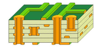
In a multi-layer PCB, there are usually signal layers (S), power (P) planes, and ground (GND) planes.
The power plane and ground plane are usually undivided solid planes, which will provide a good low-impedance current return path for the current of adjacent signal traces. Most of the signal layer is located between these power or ground reference plane layers, forming a symmetrical stripline or an asymmetrical stripline.
The top and bottom layers of a multilayer PCB are usually used to place components and a small number of traces. These signal traces are not required to be too long to reduce the direct radiation generated by the traces.
(2). Determine the single power reference plane (power plane)
Using decoupling capacitors is an important measure to solve the power integrity problem. Decoupling capacitors can only be placed on the top and bottom layers of the PCB.
The traces, pads, and vias of the decoupling capacitors will seriously affect the effect of the decoupling capacitors. This requires that the traces connecting the decoupling capacitors should be as short and wide as possible, and the wires connected to the vias should also be as short as possible.
For example, in a high-speed digital circuit, the decoupling capacitors can be placed on the top layer of the PCB, the second layer can be assigned to the high-speed digital circuit (such as the processor) as the power layer, the third layer can be used as the signal layer, and the fourth layer can be set as the high-speed digital circuit ground.
In addition, it is necessary to try to ensure that the signal traces driven by the same high-speed digital device use the same power layer as the reference plane, and this power layer is the power supply layer of the high-speed digital device.
(3). Determine the multiple power reference planes
The multiple power reference planes will be divided into several physical areas with different voltages. If the signal layer is close to the multiple power layer, the signal current on the signal layer near it will encounter an undesirable return path, causing gaps in the return path. For high-speed digital signals, this unreasonable return path design may cause serious problems, so it is required that high-speed digital signal wiring should be away from the multiple power reference planes.
(4). Determine multiple ground reference planes (ground planes)
Multiple ground reference planes (ground layers) can provide a good low-impedance current return path and reduce common-mode EMl.
The ground plane and the power plane should be tightly coupled, and the signal layer should also be tightly coupled with the adjacent reference plane. This goal can be achieved by reducing the dielectric thickness between layers.
(5). Reasonable design of wiring combinations
The two layers spanned by a signal path are called a “wiring combination”. The best wiring combination design is to avoid the return current flowing from one reference plane to another, but to flow from one point (plane) to another point (plane) on a reference plane. In order to complete complex wiring, inter-layer conversion of routing is inevitable.
When switching between signal layers, it is necessary to ensure that the return current can flow smoothly from one reference plane to another. In a design, it is reasonable to treat adjacent layers as a wiring combination.
If a signal path needs to cross multiple layers, it is usually not a reasonable design to treat it as a wiring combination, because a path passing through multiple layers is not smooth for the return current. Although the ground bounce can be reduced by placing decoupling capacitors near the vias or reducing the dielectric thickness between the reference planes, it is not a good design.
(6). Set the wiring direction
On the same signal layer, it should be ensured that the direction of most wiring is consistent and should be orthogonal to the wiring direction of the adjacent signal layer.
For example, the wiring direction of one signal layer can be set to the “Y-axis” direction, and the wiring direction of another adjacent signal layer can be set to the “X-axis” direction.
(7). Use an even-numbered layer structure
From the designed PCB stackup, it can be found that the classic stackup design is almost all even-numbered layers, not odd-numbered layers. This phenomenon is caused by many factors, as shown below.
From the manufacturing process of printed circuit boards, we can know that all the conductive layers in the circuit board are saved on the core layer.
The material of the core layer is generally a double-sided cover board. When the core layer is fully utilized, the number of conductive layers of the printed circuit board is an even number.
Even-layer printed circuit boards have cost advantages. Due to one less layer of dielectric and copper cladding, the cost of raw materials for odd-layer printed circuit boards is slightly lower than that of even-layer printed circuit boards.
However, because odd-layer printed circuit boards need to add a non-standard laminated core layer bonding process on the basis of the core layer structure process, the processing cost of odd-layer printed circuit boards is significantly higher than that of even-layer printed circuit boards. Compared with ordinary core layer structures, adding copper cladding outside the core layer structure will lead to a decrease in production efficiency and a longer production cycle.\
Before lamination and bonding, the outer core layer also requires additional process treatment, which increases the risk of scratches and incorrect etching of the outer layer. The added outer layer treatment will greatly increase the manufacturing cost.
When the printed circuit board is in the multi-layer circuit bonding process, when its inner and outer layers are cooled, different lamination tensions will cause different degrees of bending on the printed circuit board.
Moreover, as the thickness of the circuit board increases, the risk of bending of the composite printed circuit board with two different structures increases. Odd-numbered circuit boards are prone to bending, while even-numbered printed circuit boards can avoid bending.
When designing, if there is an odd-numbered stack, the following method can be used to increase the number of layers.
If the power layer of the designed printed circuit board is an even number and the signal layer is an odd number, the method of adding a signal layer can be used. The added signal layer will not lead to an increase in cost, but can shorten the processing time and improve the quality of the printed circuit board.
If the power layer of the designed printed circuit board is an odd number and the signal layer is an even number, the method of adding a power layer can be used. Another simple method is to add a ground layer in the middle of the stack without changing other settings, that is, first lay out the odd-numbered printed circuit board, and then copy a ground layer in the middle.
In microwave circuits and mixed-medium (medium with different dielectric constants) circuits, a blank signal layer can be added close to the center of the printed circuit board stack to minimize stack imbalance.
(8). Cost considerations
In terms of manufacturing cost, with the same PCB area, the cost of a multi-layer circuit board is definitely higher than that of a single-layer or double-layer circuit board, and the more layers, the higher the cost.
However, when considering factors such as realizing circuit functions and miniaturization of circuit boards, ensuring signal integrity, EMl, EMC and other performance indicators, multi-layer circuit boards should be used as much as possible.
Comprehensive evaluation shows that the cost difference between multi-layer circuit boards and single-layer and double-layer circuit boards is not much higher than expected.