Multilayer pcb design rules
Importance Of Layer Stackup In Multilayer PCB Design
In the realm of electronics, multilayer printed circuit boards (PCBs) have become indispensable due to their ability to accommodate complex circuitry within a compact space. A critical aspect of multilayer PCB design is the layer stackup, which plays a pivotal role in determining the performance, reliability, and manufacturability of the final product. Understanding the importance of layer stackup in multilayer PCB design is essential for engineers and designers aiming to optimize their designs for both functionality and cost-effectiveness.
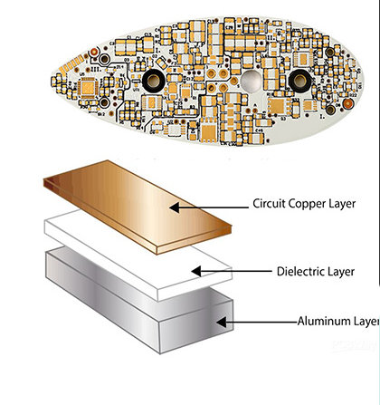
To begin with, the layer stackup refers to the arrangement and sequence of conductive and insulating layers within a PCB.
This configuration is crucial because it directly influences the electrical characteristics of the board, such as impedance, signal integrity, and electromagnetic compatibility. By carefully selecting the number and order of layers, designers can control these parameters to meet specific design requirements. For instance, a well-planned stackup can minimize signal crosstalk and electromagnetic interference, which are common challenges in high-speed digital circuits.
Moreover, the layer stackup affects the thermal management of the PCB.
As electronic components become more powerful, they generate more heat, which must be efficiently dissipated to prevent damage and ensure reliable operation. A thoughtfully designed stackup can enhance heat dissipation by incorporating thermal vias and strategically placing ground and power planes. This not only improves the thermal performance of the board but also extends the lifespan of the components mounted on it.
In addition to electrical and thermal considerations, the mechanical properties of the PCB are also influenced by the layer stackup.
The choice of materials and the arrangement of layers determine the board’s rigidity, flexibility, and overall durability. For applications that require bending or flexing, such as wearable electronics, a flexible stackup design is essential. Conversely, for applications demanding high mechanical strength, a rigid stackup with thicker core materials may be more appropriate.
Transitioning to the manufacturing perspective, the layer stackup significantly impacts the fabrication process and associated costs.
A complex stackup with numerous layers and intricate designs can increase manufacturing difficulty, leading to higher production costs and longer lead times. Therefore, designers must strike a balance between achieving the desired electrical performance and maintaining manufacturability. Collaborating with manufacturers early in the design process can help identify potential challenges and optimize the stackup for efficient production.
Furthermore, the layer stackup is integral to the assembly and testing phases of PCB production.
A well-defined stackup facilitates easier assembly by providing clear guidelines for component placement and soldering. It also aids in testing by ensuring that test points and access points are accessible, allowing for thorough inspection and quality assurance. This is particularly important in industries where reliability and safety are paramount, such as aerospace and medical devices.
In conclusion, the importance of layer stackup in multilayer PCB design cannot be overstated. It is a multifaceted aspect that influences the electrical, thermal, mechanical, and manufacturing characteristics of the board. By carefully considering the stackup during the design phase, engineers can enhance the performance and reliability of their PCBs while optimizing for cost and manufacturability. As technology continues to advance, the role of layer stackup in PCB design will remain a critical factor in meeting the ever-evolving demands of modern electronic applications.
Key Design Rules For Signal Integrity In Multilayer PCBs
In the realm of modern electronics, multilayer printed circuit boards (PCBs) have become indispensable due to their ability to support complex circuitry within a compact form factor. As devices become increasingly sophisticated, ensuring signal integrity in multilayer PCBs is paramount. Signal integrity refers to the preservation of the quality of electrical signals as they traverse the PCB, and it is crucial for the reliable performance of electronic devices. To achieve optimal signal integrity, several key design rules must be adhered to during the design and manufacturing process of multilayer PCBs.
Firstly, the stack-up configuration of a multilayer PCB plays a critical role in maintaining signal integrity.
A well-planned stack-up minimizes electromagnetic interference (EMI) and crosstalk between layers. Typically, a balanced stack-up with alternating signal and ground planes is recommended. This configuration not only provides a return path for signals but also reduces the loop area, thereby minimizing inductance and enhancing signal quality. Moreover, the use of dedicated power and ground planes helps in stabilizing the power distribution network, which is essential for maintaining signal integrity.
Transitioning to trace routing, it is imperative to consider the impedance control of signal traces.
Impedance mismatches can lead to signal reflections, which degrade signal quality. To mitigate this, designers must ensure that the trace width, spacing, and dielectric material are carefully selected to match the characteristic impedance of the transmission line. Additionally, maintaining consistent trace geometry across layers is crucial to avoid impedance discontinuities. Employing differential pairs for high-speed signals is another effective strategy, as it helps in reducing EMI and improving signal integrity.
Furthermore, via design is another aspect that significantly impacts signal integrity in multilayer PCBs.
Vias, which are used to connect traces between different layers, can introduce parasitic inductance and capacitance, leading to signal degradation. To minimize these effects, it is advisable to use blind or buried vias instead of through-hole vias, as they reduce the via stub length and associated parasitics. Additionally, ensuring that vias are properly back-drilled can further enhance signal integrity by eliminating unnecessary via stubs.
In addition to these considerations, the placement of components on a multilayer PCB is crucial for maintaining signal integrity.
Components should be strategically placed to minimize the length of critical signal paths, thereby reducing the potential for signal degradation. Moreover, sensitive components should be isolated from sources of EMI, such as power supply circuits, to prevent interference. Utilizing ground planes as shields between signal layers can also help in mitigating EMI and preserving signal quality.
Lastly, the choice of materials used in the construction of multilayer PCBs can have a profound impact on signal integrity.
High-frequency applications require materials with low dielectric loss and stable dielectric constants to ensure minimal signal attenuation. Selecting materials with these properties can significantly enhance the performance of high-speed circuits.
In conclusion, maintaining signal integrity in multilayer PCBs is a multifaceted challenge that requires careful consideration of various design rules. By optimizing stack-up configurations, controlling trace impedance, designing effective vias, strategically placing components, and selecting appropriate materials, designers can ensure that their multilayer PCBs deliver reliable performance. As electronic devices continue to evolve, adhering to these key design rules will remain essential for achieving superior signal integrity in multilayer PCBs.
Thermal Management Strategies In Multilayer PCB Design
In the realm of multilayer printed circuit board (PCB) design, thermal management emerges as a critical consideration, given the increasing complexity and density of modern electronic devices. As electronic components become more powerful and compact, the heat generated within these systems can pose significant challenges, potentially affecting performance and reliability. Therefore, effective thermal management strategies are essential to ensure the longevity and efficiency of multilayer PCBs.
To begin with, understanding the sources of heat within a multilayer PCB is crucial.
Heat is primarily generated by active components such as integrated circuits (ICs), power transistors, and other semiconductor devices. As these components operate, they dissipate energy in the form of heat, which must be efficiently managed to prevent overheating. Consequently, designers must consider the thermal characteristics of each component and the overall system during the design phase.
One fundamental strategy in thermal management is the use of thermal vias.
These are small, plated holes that connect different layers of the PCB, allowing heat to be conducted away from hot components to cooler areas or to a heat sink. By strategically placing thermal vias beneath or around heat-generating components, designers can significantly enhance heat dissipation. Moreover, the use of multiple thermal vias can further improve thermal conductivity, thereby reducing the thermal resistance of the PCB.
In addition to thermal vias, the selection of appropriate materials plays a pivotal role in thermal management.
The choice of substrate material, for instance, can greatly influence the thermal performance of a multilayer PCB. Materials with high thermal conductivity, such as metal-core PCBs or those with ceramic substrates, can effectively dissipate heat. Furthermore, the use of copper planes within the PCB layers can also aid in spreading heat evenly across the board, minimizing hotspots and ensuring uniform temperature distribution.
Another effective approach involves optimizing the layout of the PCB.
By strategically placing components with high thermal output away from sensitive areas, designers can mitigate the risk of thermal interference. Additionally, ensuring adequate spacing between components can facilitate better airflow, which is essential for natural convection cooling. In cases where natural convection is insufficient, forced air cooling, using fans or blowers, can be employed to enhance heat dissipation.
Moreover, the integration of heat sinks and thermal pads can provide additional thermal management solutions.
Heat sinks, typically made of aluminum or copper, are attached to heat-generating components to increase the surface area for heat dissipation. Thermal pads, on the other hand, are used to fill air gaps between components and heat sinks, improving thermal conductivity. These solutions are particularly effective in applications where space constraints limit the use of larger cooling systems.
Finally, simulation and modeling tools are invaluable in the design process, allowing engineers to predict and analyze the thermal behavior of a multilayer PCB before physical prototyping.
By simulating various scenarios, designers can identify potential thermal issues and optimize their designs accordingly, ensuring that the final product meets the required thermal performance standards.
In conclusion, effective thermal management in multilayer PCB design is a multifaceted challenge that requires a comprehensive approach. By employing a combination of thermal vias, material selection, layout optimization, and additional cooling solutions, designers can successfully manage heat dissipation, thereby enhancing the performance and reliability of electronic devices. As technology continues to advance, the importance of robust thermal management strategies will only grow, underscoring the need for ongoing innovation and adaptation in PCB design practices.
Best Practices For Via Placement In Multilayer PCBs
In the realm of multilayer printed circuit board (PCB) design, the strategic placement of vias is a critical factor that can significantly influence the performance, reliability, and manufacturability of the final product. Vias, which are small conductive pathways that allow electrical connections between different layers of a PCB, play a pivotal role in the overall functionality of the board. Therefore, understanding and implementing best practices for via placement is essential for engineers and designers aiming to optimize their multilayer PCB designs.
To begin with, it is important to consider the type of vias being used.
There are several types of vias, including through-hole vias, blind vias, and buried vias, each serving distinct purposes and offering unique advantages. Through-hole vias extend through the entire board, connecting all layers, and are typically used for simple, low-cost designs. In contrast, blind vias connect an outer layer to one or more inner layers without passing through the entire board, while buried vias connect only internal layers. The choice of via type should be guided by the specific requirements of the design, such as signal integrity, space constraints, and cost considerations.
Once the appropriate via type is selected, attention must be paid to the placement of these vias.
A fundamental rule in via placement is to minimize the number of vias used. Excessive use of vias can lead to increased parasitic capacitance and inductance, which can degrade signal integrity and lead to potential performance issues. Moreover, each via introduces a potential point of failure, so minimizing their number can enhance the overall reliability of the PCB.
In addition to minimizing the number of vias, it is crucial to strategically place them to avoid interference with other components and traces.
Vias should be placed in a manner that ensures a clear and direct path for signal flow, thereby reducing the risk of crosstalk and electromagnetic interference. Furthermore, vias should be positioned to facilitate efficient thermal management. By placing vias near heat-generating components, designers can help dissipate heat more effectively, thereby enhancing the thermal performance of the PCB.
Another important consideration in via placement is the aspect ratio, which is the ratio of the via’s length to its diameter.
A high aspect ratio can complicate the manufacturing process and increase the risk of defects. Therefore, maintaining an optimal aspect ratio is essential for ensuring manufacturability and reliability. Designers should work closely with manufacturers to understand the limitations and capabilities of their fabrication processes, thereby ensuring that the via design is both practical and feasible.
Moreover, it is advisable to use via stitching and via shielding techniques where appropriate.
Via stitching involves placing multiple vias around a signal trace or plane to provide a low-impedance path for return currents, which can improve signal integrity and reduce electromagnetic interference. Similarly, via shielding can be used to protect sensitive signals from external noise by surrounding them with a ring of vias connected to a ground plane.
In conclusion, the placement of vias in multilayer PCB design is a complex task that requires careful consideration of various factors, including via type, number, placement strategy, aspect ratio, and additional techniques like via stitching and shielding. By adhering to these best practices, designers can enhance the performance, reliability, and manufacturability of their multilayer PCBs, ultimately leading to more successful and efficient electronic products.