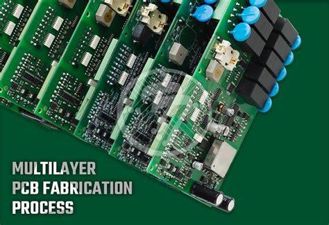
Multilayer PCB Fabrication: Core Manufacturing Steps Unveiled
Key Takeaways
When navigating PCB manufacturing for multilayer boards, understanding core technical considerations directly impacts quality and reliability. Your design choices—from precision stack-up planning to conductive layer alignment—determine how well the board manages signal integrity and electromagnetic interference (EMI). Leading PCB manufacturing companies emphasize these critical factors:
| Cost Factor | Impact Level | Optimization Strategy |
|---|---|---|
| Material Selection | High | Use cost-effective, high-Tg substrates |
| Layer Count Complexity | Critical | Balance functionality with necessity |
| Quality Control Processes | Moderate | Implement automated optical inspection |
"Proper layer arrangement isn’t just about routing—it’s a strategic shield against EMI. Always prioritize ground planes adjacent to high-speed signal layers."
– Industry Expert Tip
To minimize PCB manufacturing cost, focus on optimizing thermal stress management during lamination and ensuring cross-layer isolation through blind/buried vias. Advanced PCB manufacturing business models leverage these techniques to scale production without compromising on etching accuracy or interlayer registration. Remember: your stack-up design isn’t just a blueprint—it’s the foundation for overcoming signal degradation and heat dissipation challenges in high-density applications.
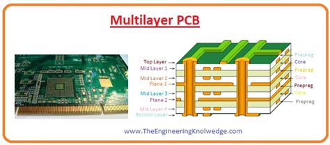
Precision Stack-Up Design Essentials
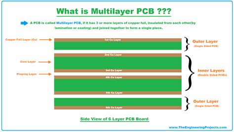
When planning PCB manufacturing for multilayer boards, your stack-up design directly impacts performance, reliability, and PCB manufacturing cost. Start by defining the layer configuration—balancing signal, power, and ground layers to optimize electrical performance. High-speed designs often require symmetrical arrangements to prevent warping during lamination, a critical consideration for PCB manufacturing companies aiming to reduce defects.
Material selection is equally vital: low-loss dielectrics minimize signal attenuation, while copper weights influence thermal management and impedance control. For instance, pairing thinner prepreg layers with thicker cores enhances interlayer bonding—key for maintaining structural integrity in high-density designs. Use simulation tools to model dielectric constants and thermal expansion coefficients, ensuring compatibility with your PCB manufacturing business workflows.
Precision alignment of conductive layers demands advanced registration systems. Even minor misalignments can cause short circuits or impedance mismatches, escalating rework costs. Collaborate closely with your fabrication partner to verify drilling tolerances and etching compensation—factors that determine final yield rates. For deeper insights into optimizing layer arrangements, explore industry-leading practices.
By prioritizing these elements, you create a foundation that streamlines subsequent steps like lamination and etching, ultimately balancing performance with PCB manufacturing cost efficiency.
Conductive Layer Alignment Techniques
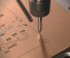
Achieving precise alignment between conductive layers is critical in PCB manufacturing, as even micron-level deviations can compromise signal integrity or create electromagnetic interference (EMI) risks. Modern PCB manufacturing companies rely on automated optical inspection (AOI) systems and laser-drilled alignment markers to ensure layers align within ±25μm tolerances. You’ll often encounter registration systems that use fiducial marks or X-ray imaging to verify layer positioning before lamination—a step that directly impacts PCB manufacturing cost by reducing material waste and rework.
For high-density designs, sequential build-up (SBU) techniques allow incremental layer alignment, minimizing cumulative errors. Advanced shops employ pattern recognition algorithms to cross-check copper traces against design files, ensuring interlayer connections remain intact. This precision becomes especially vital when balancing PCB manufacturing business priorities like scalability and reliability. Misaligned layers not only risk short circuits but also degrade impedance control, underscoring why alignment accuracy directly affects both performance and long-term operational costs. Transitioning to lamination requires maintaining this alignment through thermal cycles—a challenge addressed in the next phase of fabrication.
Advanced Lamination Process Breakdown
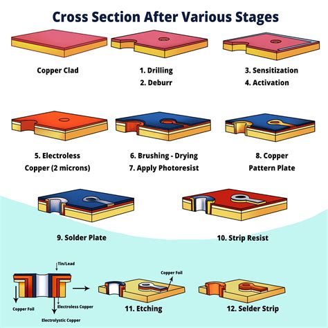
The advanced lamination process forms the structural backbone of multilayer PCB fabrication, binding conductive layers and insulating materials into a unified board. After establishing precise layer alignment, you’ll encapsulate the stack with prepreg (pre-impregnated resin) sheets, which act as both adhesive and dielectric. Critical temperature and pressure controls during pressing ensure uniform resin flow, eliminating air pockets that could compromise interlayer bonding.
Modern pcb manufacturing companies employ automated hydraulic presses with real-time monitoring to maintain optimal lamination conditions—typically 180–200°C and 300–500 psi. This phase directly impacts pcb manufacturing cost, as inefficient cycles waste energy or risk delamination. Post-lamination, the board undergoes controlled cooling to stabilize the substrate, preventing warping that might affect subsequent drilling or etching steps.
For pcb manufacturing business operators, selecting prepreg materials with compatible thermal expansion coefficients is vital. Mismatched layers can create microscopic stress points, leading to signal loss or mechanical failure. Advanced lamination also integrates hybrid materials like polyimide or ceramic-filled resins for high-frequency applications, balancing performance with scalability. By refining this step, you ensure reliable signal paths and robust interconnects, laying the groundwork for successful multilayer PCB fabrication.
Multilayer PCB Etching Best Practices
When etching conductive layers in PCB manufacturing, precision determines both performance and PCB manufacturing cost. Begin by selecting high-resolution photoresist materials to define circuit patterns accurately, as even minor deviations can compromise signal integrity. Modern PCB manufacturing companies often use laser direct imaging (LDI) to achieve micron-level accuracy, especially for dense multilayer designs.
During chemical etching, tightly control etchant concentration and temperature to maintain uniform copper removal. Over-etching risks thinning traces, while under-etching leaves conductive residues—both scenarios escalate electromagnetic interference (EMI) risks. For inner layers, ensure alignment with adjacent dielectric substrates using optical registration systems, a critical step before lamination.
Another key consideration is balancing copper thickness. Thicker copper improves current handling but requires longer etching times, increasing PCB manufacturing business overhead. Advanced facilities employ automated spray-etching systems to optimize uniformity across large panels, reducing material waste. Post-etching, conduct automated optical inspections (AOI) to detect micro-shorts or open circuits, addressing flaws before stacking layers.
Finally, integrate cross-section analysis to verify etch profiles, particularly for high-frequency designs where trapezoidal traces degrade signal quality. By refining these practices, you mitigate risks that escalate PCB manufacturing cost while ensuring compliance with industry reliability standards.
Ensuring Signal Integrity in PCBs
Maintaining signal integrity in multilayer PCBs requires meticulous attention to impedance control, material selection, and trace routing. High-speed signals demand precise impedance matching, which starts with choosing dielectric materials like FR-4 or specialized laminates with consistent dielectric constants. PCB manufacturing companies often use simulation tools to model signal paths, ensuring minimal reflection or distortion during transmission.
To avoid crosstalk, critical traces must be spaced appropriately, with ground planes acting as shields between sensitive layers. This becomes especially vital in designs where PCB manufacturing cost constraints push for tighter layouts. Differential pair routing, coupled with symmetric stack-up configurations, helps maintain balanced signal propagation while reducing electromagnetic interference.
Thermal management also plays a role—excessive heat can alter material properties, degrading signal performance over time. PCB manufacturing business practices like controlled-depth drilling and via-in-pad techniques minimize thermal stress on high-frequency paths. Additionally, advanced etching processes ensure clean trace edges, preventing impedance discontinuities that could disrupt signals.
Finally, rigorous testing—such as time-domain reflectometry (TDR)—validates signal integrity before mass production. By aligning design choices with PCB manufacturing capabilities, you ensure reliable performance in complex multilayer boards without compromising speed or accuracy.
Minimizing EMI Through Layer Arrangement
Effective layer arrangement in PCB manufacturing begins with understanding how electromagnetic interference (EMI) propagates through conductive layers. By strategically positioning ground and power planes adjacent to high-speed signal layers, you create natural shielding that absorbs or redirects unwanted electromagnetic fields. Symmetrical stack-up designs further enhance EMI suppression by balancing capacitive coupling between layers, a technique often prioritized by experienced PCB manufacturing companies to maintain signal integrity.
When planning your stack-up, place sensitive analog circuits between solid ground planes to isolate them from noisy digital sections. This separation reduces cross-talk, a common source of EMI in complex boards. For designs requiring dense routing, alternating signal layers with reference planes ensures controlled impedance paths while minimizing loop areas that radiate interference. Though advanced layer configurations may elevate PCB manufacturing cost, they prevent costly redesigns caused by EMI failures in mission-critical applications.
PCB manufacturing businesses also leverage dielectric materials with lower dissipation factors to reduce high-frequency losses, complementing smart layer arrangements. Always validate your design through electromagnetic simulation tools before finalizing the stack-up—this step identifies potential hotspots and optimizes layer spacing for EMI mitigation without compromising thermal performance. By integrating these principles, you align with industry benchmarks for EMI-resistant multilayer boards while maintaining scalability in production.
Cross-Layer Signal Isolation Methods
Achieving effective signal isolation in PCB manufacturing requires strategic layer planning and material selection. When designing multilayer boards, ground planes and shielding layers act as barriers to prevent electromagnetic coupling between adjacent conductive layers. PCB manufacturing companies often use differential pair routing combined with controlled impedance traces to minimize cross-talk, especially in high-speed applications. Implementing via stitching around sensitive signal paths further enhances isolation by creating a Faraday cage effect, redirecting interference away from critical circuits.
To balance PCB manufacturing cost and performance, dielectric materials with low dissipation factors are prioritized between high-frequency layers. This reduces signal attenuation while maintaining isolation. For power-hungry designs, dedicated power planes separated by prepreg layers help contain noise. Advanced PCB manufacturing business practices also incorporate laser-drilled microvias to isolate signals vertically, avoiding parasitic capacitance buildup. Transitioning between layers? Ensure return paths are continuous—disrupted reference planes can compromise isolation, leading to EMI leaks. By integrating these methods, you maintain signal integrity without inflating layer counts, a key consideration in cost-sensitive multilayer projects.
Thermal Stress Management Strategies
Managing thermal stress is critical in PCB manufacturing to prevent delamination, warping, or solder joint failures during operation. When designing multilayer boards, you must account for coefficient of thermal expansion (CTE) mismatches between materials like copper, prepreg, and substrates. PCB manufacturing companies often use high-Tg (glass transition temperature) laminates and low-CTE core materials to minimize dimensional instability under temperature cycling.
To optimize PCB manufacturing cost, consider embedding thermal vias or copper-balanced stacks to dissipate heat efficiently. During lamination, precise control of pressure and temperature profiles ensures even resin flow, reducing residual stress. Advanced simulation tools help predict hotspots, allowing adjustments in layer arrangement or via placement before fabrication.
For PCB manufacturing business models prioritizing reliability, implementing post-assembly thermal cycling tests is essential. These tests validate whether the board withstands repeated thermal shocks, particularly in applications like automotive or aerospace electronics. Partnering with suppliers offering CTE-matched materials can further mitigate risks while maintaining signal integrity across layers.
By integrating these strategies early in the design phase, you align thermal performance with the board’s electrical requirements, ensuring long-term durability without compromising functionality.
Conclusion
When navigating the complexities of PCB manufacturing, understanding how each fabrication step impacts performance and reliability is critical. From optimizing PCB manufacturing cost through precise stack-up design to ensuring flawless conductive layer alignment, every decision directly affects your final product’s quality. Partnering with experienced PCB manufacturing companies can streamline this process, as their expertise in advanced lamination and etching techniques minimizes errors that might otherwise escalate expenses.
For businesses scaling their PCB manufacturing business, balancing technical precision with cost-efficiency remains paramount. Techniques like cross-layer signal isolation and thermal stress management not only enhance signal integrity but also reduce long-term risks of electromagnetic interference (EMI). By prioritizing these best practices, you ensure that your multilayer PCBs meet industry standards while maintaining competitive margins. Remember, the success of your project hinges on aligning engineering rigor with strategic partnerships—a synergy that transforms intricate designs into robust, market-ready solutions.
FAQs
What distinguishes multilayer PCB manufacturing from single-layer production?
Multilayer PCB manufacturing involves bonding conductive layers with insulating material through precision lamination, requiring advanced alignment systems to ensure interlayer connectivity. Single-layer boards skip this complexity, directly affecting PCB manufacturing cost due to added materials and labor.
How do PCB manufacturing companies ensure signal integrity in multilayer designs?
Leading PCB manufacturing companies use impedance-controlled routing and cross-layer isolation techniques. They optimize stack-up configurations to minimize crosstalk while employing high-quality dielectric materials to maintain consistent electrical properties across layers.
What factors most impact PCB manufacturing cost for multilayer boards?
Key cost drivers include layer count, material grade (e.g., high-Tg FR4), and tolerances for features like microvias. PCB manufacturing business models often prioritize bulk orders to offset expenses tied to advanced processes like laser drilling or sequential lamination.
Can you reduce electromagnetic interference (EMI) without increasing layer count?
Yes. Strategic placement of ground planes and shielding layers, combined with proper via stitching, mitigates EMI. Many PCB manufacturing providers now integrate simulation tools during design reviews to preemptively address noise issues.
How do thermal stresses affect long-term reliability in multilayer PCBs?
Mismatched coefficients of thermal expansion (CTE) between materials can cause delamination. Reputable PCB manufacturing companies perform thermal cycle testing and use low-CTE substrates to ensure durability in high-temperature environments.
Optimize Your Next Multilayer PCB Design Click Here for Expert Support
For tailored solutions that balance performance and PCB manufacturing cost, connect with specialists who streamline complex layer stack-ups and material selection.