Multilayer PCB Photolithography Process: A Comprehensive Guide
Abstract
The photolithography process is a critical step in the fabrication of multilayer printed circuit boards (PCBs). It enables the precise transfer of circuit patterns onto copper-clad substrates, ensuring high-density interconnects and reliable performance in modern electronics. This article explores the photolithography process for multilayer PCBs, covering key steps, materials, challenges, and advancements in the field.
1. Introduction
Multilayer PCBs are essential components in advanced electronic devices, including smartphones, computers, and automotive systems. These boards consist of multiple conductive layers separated by insulating dielectric materials, interconnected through vias and plated through-holes (PTHs). Photolithography plays a pivotal role in defining the fine-line circuitry required for high-performance PCBs.
This article provides an in-depth analysis of the photolithography process for multilayer PCBs, discussing:
- The fundamentals of photolithography
- Key steps in the process
- Materials used (photoresists, etchants, substrates)
- Challenges and solutions
- Recent advancements
2. Fundamentals of Photolithography in PCB Manufacturing
Photolithography is a subtractive process that transfers a circuit pattern onto a copper-clad laminate using light-sensitive photoresist and chemical etching. The process involves:
- Substrate Preparation – Cleaning and surface treatment of the copper-clad laminate.
- Photoresist Application – Coating the substrate with a light-sensitive polymer.
- Exposure – Transferring the circuit pattern using UV light and a photomask.
- Development – Removing unexposed (or exposed, depending on resist type) areas to reveal the copper underneath.
- Etching – Chemically removing unwanted copper to form the circuit traces.
- Stripping – Removing the remaining photoresist to complete the patterning.
For multilayer PCBs, this process is repeated for each conductive layer before lamination.
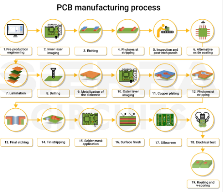
3. Step-by-Step Photolithography Process for Multilayer PCBs
3.1 Substrate Preparation
The process begins with a copper-clad laminate, typically made of FR-4 (epoxy-glass composite). Surface preparation includes:
- Mechanical Cleaning – Scrubbing to remove oxides and contaminants.
- Chemical Cleaning – Acid or alkaline treatment to enhance photoresist adhesion.
3.2 Photoresist Application
A liquid or dry film photoresist is applied to the copper surface. Two types of photoresists are commonly used:
- Positive Photoresist – Exposed areas become soluble and are removed during development.
- Negative Photoresist – Unexposed areas dissolve, leaving the exposed pattern intact.
Methods of Application:
- Spin Coating – Used for high-resolution ICs but less common in PCBs.
- Dry Film Lamination – Preferred for PCBs due to uniform thickness and ease of handling.
3.3 Exposure
The photoresist-coated substrate is exposed to UV light through a photomask (also called an artwork film). The mask contains the desired circuit pattern in opaque (blocking UV) and transparent (allowing UV) regions.
Exposure Systems:
- Contact Printing – The mask is in direct contact with the substrate (high resolution but risk of damage).
- Proximity Printing – The mask is slightly separated from the substrate (reduces defects but lowers resolution).
- Projection Printing – Uses lenses to project the pattern (high precision but expensive).
3.4 Development
After exposure, the board undergoes development, where a chemical solution (e.g., sodium carbonate for negative resist) dissolves the uncured resist, revealing the copper traces.
3.5 Etching
The exposed copper is removed using an etchant solution:
- Ferric Chloride (FeCl₃) – Traditional etchant, cost-effective but slower.
- Ammonium Persulfate – Faster etching, better for fine-line PCBs.
- Cupric Chloride (CuCl₂) – Used in industrial-scale PCB production.
3.6 Stripping
The remaining photoresist is stripped using an alkaline solution (e.g., NaOH), leaving only the desired copper circuitry.
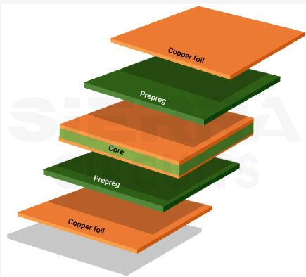
3.7 Multilayer Alignment and Lamination
For multilayer PCBs, each layer undergoes photolithography separately. After patterning, the layers are stacked, aligned, and laminated under heat and pressure. Vias are drilled and plated to establish interlayer connections.
4. Materials in PCB Photolithography
4.1 Photoresists
- Dry Film Resist (DFR) – Most common in PCBs, offers uniform thickness (15–50 µm).
- Liquid Resist – Used for ultra-fine features (< 10 µm line width).
4.2 Substrates
- FR-4 – Standard material for rigid PCBs.
- Polyimide – Used in flexible PCBs.
- High-Frequency Laminates (e.g., Rogers) – For RF/microwave applications.
4.3 Etchants
- Ferric Chloride – Economical but requires careful disposal.
- Alkaline Etchants – Used for fine-line etching in HDI (high-density interconnect) PCBs.
5. Challenges in Multilayer PCB Photolithography
5.1 Alignment Accuracy
Misalignment between layers can cause short circuits or open connections. Advanced registration systems (e.g., laser direct imaging) improve precision.
5.2 Fine-Line Resolution
As PCBs shrink, achieving sub-20µm traces becomes challenging. Solutions include:
- Laser Direct Imaging (LDI) – Eliminates photomasks, improving resolution.
- Advanced Photoresists – Higher sensitivity for finer features.
5.3 Etch Uniformity
Uneven etching can lead to undercutting or incomplete copper removal. Process control and optimized etchants mitigate this issue.
5.4 Environmental Concerns
Traditional etchants (FeCl₃) are hazardous. Eco-friendly alternatives (e.g., copper recycling etchants) are gaining traction.
6. Recent Advancements in PCB Photolithography
6.1 Laser Direct Imaging (LDI)
Replaces photomasks with laser exposure, enabling finer features (< 10 µm) and faster prototyping.
6.2 Semi-Additive Process (SAP)
Used in HDI PCBs, SAP involves:
- Electroless copper deposition on a substrate.
- Photolithography to define traces.
- Electroplating to build up copper.
- Etching away excess copper.
6.3 Nanotechnology in Photoresists
Nanoparticle-enhanced resists improve resolution and durability for next-gen PCBs.
6.4 AI-Driven Process Optimization
Machine learning algorithms optimize exposure and etching parameters, reducing defects.
7. Conclusion
Photolithography remains a cornerstone of multilayer PCB manufacturing, enabling the miniaturization and high performance of modern electronics. Advances in LDI, eco-friendly etchants, and high-resolution photoresists continue to push the boundaries of PCB technology. As demand for smaller, faster, and more reliable PCBs grows, further innovations in photolithography will be essential.