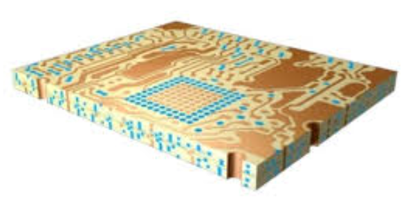
Multilayer pcb production
Advantages Of Multilayer PCB Over Single And Double-Layer PCBs
Multilayer printed circuit boards (PCBs) have become increasingly prevalent in modern electronics, offering a range of advantages over their single and double-layer counterparts. As technology continues to advance, the demand for more compact, efficient, and high-performance electronic devices has driven the adoption of multilayer PCBs. These advanced circuit boards consist of multiple layers of conductive material, typically copper, separated by insulating layers, which are laminated together to form a single, cohesive unit. This construction method provides several key benefits that make multilayer PCBs the preferred choice for many applications.
One of the primary advantages of multilayer PCBs is their ability to support higher component density.
By stacking multiple layers, designers can incorporate more electronic components within a smaller footprint. This is particularly beneficial in the development of compact devices such as smartphones, tablets, and wearable technology, where space is at a premium. The increased component density also allows for more complex circuitry, enabling the creation of sophisticated electronic systems that would be impossible to achieve with single or double-layer PCBs.
In addition to supporting higher component density, multilayer PCBs offer improved electrical performance.
The close proximity of the layers allows for shorter and more direct interconnections between components, which reduces the length of signal paths. This, in turn, minimizes signal loss and electromagnetic interference (EMI), leading to better signal integrity and faster signal transmission. Consequently, multilayer PCBs are ideal for high-speed and high-frequency applications, such as telecommunications, computing, and advanced medical devices, where reliable and efficient signal transmission is critical.
Another significant advantage of multilayer PCBs is their enhanced thermal management capabilities.
The multiple layers provide additional pathways for heat dissipation, which helps to prevent overheating and ensures the stable operation of electronic components. This is particularly important in high-power applications, such as power supplies and automotive electronics, where effective thermal management is essential to maintain performance and longevity. Furthermore, the use of advanced materials and design techniques in multilayer PCBs can further enhance their thermal performance, making them suitable for even the most demanding environments.
Moreover, multilayer PCBs offer greater design flexibility compared to single and double-layer boards.
The ability to incorporate multiple layers allows designers to create more intricate and optimized circuit layouts, which can improve overall system performance and functionality. This flexibility also enables the integration of various features, such as embedded components and advanced interconnects, which can further enhance the capabilities of the final product. Additionally, the use of computer-aided design (CAD) tools and advanced manufacturing techniques has made it easier to design and produce multilayer PCBs, reducing development time and costs.
While the advantages of multilayer PCBs are clear, it is important to acknowledge that their production can be more complex and costly compared to single and double-layer boards.
The manufacturing process requires precise alignment and lamination of the layers, as well as advanced inspection and testing methods to ensure quality and reliability. However, the benefits of improved performance, higher component density, and enhanced thermal management often outweigh the additional costs, making multilayer PCBs a worthwhile investment for many applications.
In conclusion, multilayer PCBs offer numerous advantages over single and double-layer boards, including higher component density, improved electrical performance, enhanced thermal management, and greater design flexibility. These benefits make them the preferred choice for a wide range of modern electronic devices and systems, driving innovation and enabling the development of more advanced and efficient technologies. As the demand for high-performance electronics continues to grow, the adoption of multilayer PCBs is likely to increase, further solidifying their importance in the field of electronics manufacturing.
Key Steps In The Multilayer PCB Manufacturing Process
The production of multilayer printed circuit boards (PCBs) is a complex and intricate process that requires precision and attention to detail. This process begins with the design phase, where engineers use specialized software to create a detailed blueprint of the PCB. This blueprint includes the layout of the various layers, the placement of components, and the routing of electrical connections. Once the design is finalized, it is converted into a format that can be used by the manufacturing equipment.
Following the design phase, the next step is the creation of the individual layers.
Each layer is made from a thin sheet of conductive material, typically copper, which is laminated onto a non-conductive substrate. The copper is then etched away to create the desired circuit pattern. This etching process is repeated for each layer, with the patterns on each layer carefully aligned to ensure proper electrical connections.
After the individual layers are created, they are stacked together to form the multilayer PCB.
This stacking process is critical, as any misalignment can result in faulty connections and a non-functional PCB. To ensure proper alignment, the layers are often pinned together and then subjected to a process called lamination. During lamination, the stack of layers is heated and pressed together, causing the layers to bond and form a single, solid board.
Once the layers are laminated, the next step is drilling.
Holes are drilled through the board to create vias, which are used to connect the different layers electrically. These holes are then plated with a conductive material, typically copper, to ensure a reliable electrical connection. The drilling process must be precise, as any deviation can result in misaligned vias and a non-functional PCB.
Following the drilling and plating process, the board undergoes a series of inspections and tests to ensure its quality and functionality.
These inspections include visual checks, automated optical inspection (AOI), and electrical testing. Visual checks are used to identify any obvious defects, such as misaligned layers or incomplete etching. AOI uses cameras and software to inspect the board for more subtle defects, such as short circuits or open circuits. Electrical testing involves applying a voltage to the board and measuring the resulting current to ensure that all connections are functioning correctly.
Once the board has passed all inspections and tests, it is ready for the final steps of the manufacturing process.
These steps include solder mask application, silkscreen printing, and surface finish application. The solder mask is a protective layer that is applied to the board to prevent solder bridges and short circuits during the assembly process. The silkscreen is used to print labels and markings on the board, which help with component placement and identification. The surface finish is applied to the exposed copper areas to protect them from oxidation and ensure good solderability.
In conclusion, the production of multilayer PCBs involves a series of precise and carefully controlled steps, from design and layer creation to lamination, drilling, inspection, and final finishing. Each step is critical to ensuring the quality and functionality of the final product. By following these key steps, manufacturers can produce reliable and high-performance multilayer PCBs that meet the demanding requirements of modern electronic devices.
Common Challenges In Multilayer PCB Design And How To Overcome Them
Multilayer PCB production is a sophisticated process that involves the integration of multiple layers of electronic circuits into a single board. This complexity introduces several challenges that designers must navigate to ensure the final product meets the desired specifications. One of the primary challenges in multilayer PCB design is managing signal integrity. As the number of layers increases, so does the potential for signal interference and crosstalk between adjacent layers. To mitigate this, designers often employ techniques such as careful layer stacking and the use of ground planes to isolate signals. Additionally, maintaining consistent impedance across traces is crucial, which can be achieved through meticulous trace width and spacing calculations.
Another significant challenge is thermal management.
Multilayer PCBs, due to their dense circuitry, can generate substantial heat, which, if not properly managed, can lead to component failure or reduced performance.
Effective thermal management strategies include the use of thermal vias, which help dissipate heat through the layers, and the incorporation of heat sinks or thermal pads. Moreover, selecting materials with high thermal conductivity can enhance heat dissipation, ensuring the PCB operates within safe temperature ranges.
Furthermore, the complexity of multilayer PCB design often leads to difficulties in ensuring manufacturability.
As designs become more intricate, the risk of manufacturing defects such as misalignments, incomplete connections, or delamination increases. To overcome these issues, designers must collaborate closely with manufacturers during the design phase, adhering to design for manufacturability (DFM) guidelines. This collaboration helps identify potential issues early and allows for adjustments that facilitate smoother production processes.
In addition to manufacturability, the aspect of testing and validation poses its own set of challenges.
Multilayer PCBs require rigorous testing to ensure all layers function correctly and that there are no hidden defects. Traditional testing methods may not be sufficient, necessitating advanced techniques such as automated optical inspection (AOI) and X-ray inspection. These methods allow for thorough examination of the internal layers and connections, ensuring the integrity of the PCB before it moves to the next stage of production.
Moreover, the aspect of design complexity cannot be overlooked.
As the number of layers increases, so does the complexity of routing and placement of components. This complexity can lead to longer design cycles and increased potential for errors. Utilizing advanced design software that offers features like auto-routing and real-time error checking can significantly streamline the design process. Additionally, adopting a modular design approach, where the PCB is divided into smaller, manageable sections, can simplify the overall design and reduce the likelihood of errors.
Lastly, cost considerations are a perennial challenge in multilayer PCB production.
The materials and processes involved in creating multilayer PCBs are inherently more expensive than those for single-layer boards. To manage costs effectively, designers must strike a balance between performance requirements and budget constraints. This can involve selecting cost-effective materials that still meet performance criteria or optimizing the layer count to reduce material usage without compromising functionality.
In conclusion, while multilayer PCB design presents numerous challenges, these can be effectively managed through a combination of strategic design practices, close collaboration with manufacturers, and the use of advanced testing and design tools. By addressing issues related to signal integrity, thermal management, manufacturability, testing, design complexity, and cost, designers can overcome the hurdles associated with multilayer PCB production and deliver high-quality, reliable products.
Innovations In Multilayer PCB Materials And Technologies
The production of multilayer printed circuit boards (PCBs) has undergone significant advancements in recent years, driven by the increasing demand for more compact, efficient, and high-performance electronic devices. Innovations in materials and technologies have played a crucial role in enhancing the capabilities of multilayer PCBs, making them indispensable in various industries, including telecommunications, aerospace, and consumer electronics. As we delve into these innovations, it becomes evident that the evolution of multilayer PCB production is a testament to the relentless pursuit of excellence in electronic manufacturing.
One of the most notable advancements in multilayer PCB production is the development of high-performance materials.
Traditional materials such as FR-4, a composite of woven fiberglass cloth with an epoxy resin binder, have been the industry standard for many years. However, the limitations of FR-4, particularly in high-frequency applications, have necessitated the exploration of alternative materials. Consequently, materials such as polyimide, PTFE (polytetrafluoroethylene), and ceramic-filled laminates have gained prominence. These materials offer superior thermal stability, lower dielectric constants, and reduced signal loss, making them ideal for high-speed and high-frequency applications.
In addition to material innovations, advancements in fabrication technologies have significantly impacted multilayer PCB production.
One such technology is the use of laser drilling for via formation. Traditional mechanical drilling methods often struggle with the precision required for microvias, especially as the number of layers in a PCB increases. Laser drilling, on the other hand, provides unparalleled accuracy and can create vias with diameters as small as 20 micrometers. This precision is crucial for maintaining signal integrity and ensuring reliable interconnections between layers.
Moreover, the advent of advanced plating techniques has further enhanced the reliability and performance of multilayer PCBs.
Electroless copper plating, for instance, has become a preferred method for creating uniform and consistent copper layers on the PCB substrate. This technique ensures excellent adhesion and conductivity, which are essential for the overall performance of the PCB. Additionally, the use of advanced surface finishes such as immersion gold and organic solderability preservatives (OSPs) has improved the solderability and longevity of PCBs, making them more robust and durable.
Another significant innovation in multilayer PCB production is the integration of embedded components. Traditionally, passive components such as resistors and capacitors are mounted on the surface of the PCB. However, embedding these components within the PCB layers can save valuable surface space and reduce the overall size of the device. This approach not only enhances the functionality of the PCB but also improves its thermal management and electrical performance. The development of advanced embedding techniques, such as laser direct structuring (LDS) and additive manufacturing, has made it possible to integrate components seamlessly into the PCB structure.
Furthermore, the implementation of advanced design software has revolutionized the way multilayer PCBs are designed and manufactured.
Computer-aided design (CAD) tools now offer sophisticated features such as 3D modeling, signal integrity analysis, and thermal simulation. These tools enable designers to optimize the layout and performance of multilayer PCBs, ensuring that they meet the stringent requirements of modern electronic devices. The integration of design and manufacturing processes through digital twins and Industry 4.0 technologies has also streamlined production, reducing lead times and improving overall efficiency.
In conclusion, the innovations in multilayer PCB materials and technologies have significantly advanced the capabilities of electronic devices. High-performance materials, precision fabrication techniques, advanced plating methods, embedded components, and sophisticated design software have all contributed to the evolution of multilayer PCB production. As the demand for more compact, efficient, and high-performance electronic devices continues to grow, these innovations will undoubtedly play a pivotal role in shaping the future of electronic manufacturing.