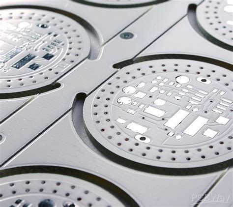
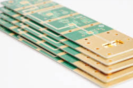
Multilayer printed circuit board process
Design Considerations For Multilayer Printed Circuit Boards
Designing multilayer printed circuit boards (PCBs) involves a complex interplay of various factors that must be meticulously considered to ensure optimal performance and reliability.
One of the primary considerations is the layer stack-up, which refers to the arrangement of conductive and insulating layers within the PCB.
The stack-up not only affects the electrical performance but also influences the mechanical strength and thermal management of the board. Therefore, selecting the appropriate number of layers and their configuration is crucial. Typically, a balanced stack-up is preferred to minimize warping and ensure uniform thickness.
Another critical aspect is the selection of materials.
The choice of dielectric materials, such as FR4, polyimide, or Rogers, impacts the board’s electrical properties, including signal integrity and impedance control. The dielectric constant and loss tangent of the material must be carefully matched to the application’s requirements. Additionally, the copper thickness for each layer must be determined based on current-carrying capacity and thermal considerations. Thicker copper layers can handle higher currents but may complicate the manufacturing process and increase costs.
Signal integrity is a paramount concern in multilayer PCB design.
High-speed signals are susceptible to issues such as crosstalk, signal reflection, and electromagnetic interference (EMI). To mitigate these problems, designers often employ techniques such as controlled impedance routing, differential pair routing, and the use of ground planes. Ground planes provide a return path for signals, reducing EMI and improving signal integrity. Moreover, careful placement of decoupling capacitors near power pins can help stabilize voltage levels and filter out noise.
Thermal management is another vital consideration.
As electronic components become more powerful, they generate more heat, which must be efficiently dissipated to prevent damage and ensure reliable operation. Thermal vias, heat sinks, and thermal pads are commonly used to enhance heat dissipation. Additionally, the layout should be designed to facilitate airflow and minimize hotspots. Thermal simulations can be conducted during the design phase to predict and address potential thermal issues.
Manufacturability is an essential factor that cannot be overlooked.
The design must comply with the capabilities and limitations of the PCB manufacturer. This includes considerations such as minimum trace width and spacing, via sizes, and aspect ratios. Design for manufacturability (DFM) guidelines should be followed to ensure that the board can be produced reliably and cost-effectively. Collaboration with the manufacturer during the design phase can help identify potential issues early and avoid costly revisions.
Testing and validation are crucial steps in the design process.
Once the PCB is fabricated, it must undergo rigorous testing to verify its performance and reliability. This includes electrical testing to check for continuity and shorts, as well as functional testing to ensure that the board operates as intended. In some cases, environmental testing may be required to assess the board’s performance under various conditions, such as temperature extremes and humidity.
In conclusion, designing multilayer printed circuit boards is a multifaceted process that requires careful consideration of various factors, including layer stack-up, material selection, signal integrity, thermal management, manufacturability, and testing. By addressing these considerations systematically, designers can create PCBs that meet the stringent demands of modern electronic applications, ensuring both performance and reliability.
Manufacturing Steps In Multilayer PCB Fabrication
The manufacturing process of multilayer printed circuit boards (PCBs) is a complex and meticulous procedure that involves several critical steps to ensure the final product meets the required specifications and performance standards. Initially, the process begins with the design phase, where engineers create detailed schematics and layout designs using specialized software. These designs are then converted into a format suitable for manufacturing, typically Gerber files, which contain all the necessary information about the PCB layers, traces, and components.
Following the design phase, the next step is the preparation of the raw materials.
This involves selecting high-quality substrates, usually made of fiberglass-reinforced epoxy resin, known as FR4. The substrates are then coated with a thin layer of copper on both sides, which will form the conductive pathways of the PCB. Once the materials are prepared, the process moves on to the inner layer imaging.
During inner layer imaging, the design patterns for the inner layers are transferred onto the copper-clad substrates using a photolithographic process.
A photosensitive resist is applied to the copper surface, and the design is exposed onto the resist using ultraviolet light. The exposed areas of the resist harden, while the unexposed areas remain soft and are subsequently removed, revealing the copper underneath. The exposed copper is then etched away using a chemical solution, leaving behind the desired circuit patterns.
After the inner layers are etched, they undergo an inspection process to ensure accuracy and quality.
Any defects or inconsistencies are identified and corrected before proceeding to the next step, which is the lamination process. During lamination, the individual layers of the PCB are stacked together, with insulating layers of prepreg material placed between them. The stack is then subjected to high pressure and temperature in a lamination press, causing the prepreg to melt and bond the layers together into a single, solid structure.
Once the lamination is complete, the next step is drilling.
Precision drilling machines create holes for vias, which are used to connect the different layers of the PCB electrically. These holes are then plated with copper through an electroplating process, ensuring a reliable electrical connection between the layers. Following drilling and plating, the outer layers of the PCB are imaged and etched in a similar manner to the inner layers, creating the external circuit patterns.
The next phase involves applying a solder mask to the PCB.
The solder mask is a protective layer that covers the copper traces, preventing oxidation and short circuits during soldering. The solder mask is applied using a screen-printing process and then cured using ultraviolet light. After the solder mask is applied, a silkscreen layer is added, which contains labels and markings to assist with component placement and identification.
Finally, the PCB undergoes surface finishing, where a protective coating is applied to the exposed copper areas to enhance solderability and prevent corrosion.
Common surface finishes include HASL (Hot Air Solder Leveling), ENIG (Electroless Nickel Immersion Gold), and OSP (Organic Solderability Preservative). The completed PCB is then subjected to rigorous testing, including electrical testing and inspection, to ensure it meets all design specifications and quality standards.
In conclusion, the manufacturing steps in multilayer PCB fabrication are intricate and require precise control at each stage to produce a high-quality product. From design and material preparation to imaging, lamination, drilling, and finishing, each step is crucial in creating a reliable and efficient multilayer PCB.
Common Challenges In Multilayer PCB Production
The production of multilayer printed circuit boards (PCBs) is a complex process that involves several intricate steps, each of which presents its own set of challenges. One of the primary difficulties encountered in multilayer PCB production is ensuring precise alignment of the various layers. As the number of layers increases, the potential for misalignment grows, which can lead to electrical shorts or open circuits. To mitigate this issue, manufacturers employ advanced registration systems and optical alignment techniques, yet even with these technologies, achieving perfect alignment remains a formidable task.
Another significant challenge is the management of thermal stresses.
During the manufacturing process, PCBs are subjected to various thermal cycles, including lamination, soldering, and reflow processes. These thermal cycles can induce stress within the board, potentially leading to warping or delamination. To address this, manufacturers must carefully select materials with compatible thermal expansion coefficients and employ precise temperature control throughout the production process. However, even with meticulous planning, thermal stress remains a persistent concern.
Furthermore, the aspect of via formation in multilayer PCBs introduces additional complexity.
Vias, which are small holes that allow electrical connections between layers, must be drilled with extreme precision. The drilling process must ensure that the vias are correctly positioned and that their walls are smooth to facilitate reliable electrical connections. Laser drilling and mechanical drilling are commonly used techniques, but each has its limitations. Laser drilling offers high precision but can be costly, while mechanical drilling is more economical but may not achieve the same level of accuracy.
In addition to these technical challenges, the aspect of signal integrity is a critical consideration in multilayer PCB production.
As electronic devices become more sophisticated, the demand for high-speed data transmission increases. Ensuring signal integrity involves managing factors such as impedance control, crosstalk, and electromagnetic interference (EMI). Manufacturers must carefully design the PCB layout to minimize these issues, often employing techniques such as differential signaling and shielding. Despite these efforts, maintaining signal integrity in densely packed multilayer PCBs remains a challenging endeavor.
Moreover, the aspect of material selection plays a crucial role in the production of multilayer PCBs.
The choice of substrate material, copper foil, and dielectric layers can significantly impact the board’s performance and reliability. High-frequency applications, for instance, require materials with low dielectric loss and stable dielectric constants. However, these specialized materials can be expensive and may pose additional processing challenges. Balancing performance requirements with cost considerations is a constant challenge for manufacturers.
Additionally, the aspect of quality control is paramount in multilayer PCB production.
Given the complexity of these boards, thorough inspection and testing are essential to ensure that they meet the required specifications. Automated optical inspection (AOI), X-ray inspection, and electrical testing are commonly employed methods. However, detecting defects in multilayer PCBs can be more challenging than in single-layer boards due to the increased density and complexity. Ensuring comprehensive quality control without significantly increasing production time and cost is a delicate balance that manufacturers must achieve.
In conclusion, the production of multilayer printed circuit boards involves navigating a myriad of challenges, from precise layer alignment and thermal stress management to via formation and signal integrity. Material selection and quality control further complicate the process, requiring manufacturers to employ advanced techniques and technologies. Despite these challenges, the demand for multilayer PCBs continues to grow, driven by the increasing complexity and performance requirements of modern electronic devices. As such, ongoing innovation and refinement in production processes are essential to meet the evolving needs of the industry.
Quality Control Techniques For Multilayer PCBs
Quality control is a critical aspect of the manufacturing process for multilayer printed circuit boards (PCBs). Ensuring the reliability and performance of these complex electronic components requires a meticulous approach to quality assurance. Various techniques are employed to maintain the highest standards throughout the production cycle, from initial design to final inspection.
One of the primary quality control techniques used in the production of multilayer PCBs is automated optical inspection (AOI).
This method involves the use of high-resolution cameras to capture detailed images of the PCB layers. These images are then compared to the original design specifications to identify any discrepancies, such as misaligned components, missing parts, or soldering defects. AOI is particularly effective in detecting surface-level issues early in the manufacturing process, thereby reducing the likelihood of more significant problems arising later.
In addition to AOI, X-ray inspection is another vital technique for ensuring the quality of multilayer PCBs.
This method allows for the examination of internal layers and connections that are not visible to the naked eye. By using X-ray imaging, manufacturers can detect hidden defects such as voids, cracks, or misaligned vias. This non-destructive testing method is essential for verifying the integrity of the internal structure of the PCB, which is crucial for its overall performance and reliability.
Electrical testing is also a fundamental aspect of quality control for multilayer PCBs.
This process involves subjecting the PCB to various electrical tests to ensure that it meets the required performance standards. Continuity testing, for example, checks for open or short circuits within the PCB, while impedance testing verifies that the electrical resistance of the board is within acceptable limits. These tests are crucial for identifying potential issues that could affect the functionality of the final product.
Thermal cycling is another important quality control technique used in the production of multilayer PCBs.
This process involves subjecting the PCB to extreme temperature variations to assess its ability to withstand thermal stress. By exposing the board to repeated cycles of heating and cooling, manufacturers can identify potential weaknesses in the materials or construction that could lead to failure under real-world operating conditions. Thermal cycling is particularly important for PCBs used in applications where they will be exposed to fluctuating temperatures, such as in automotive or aerospace industries.
Furthermore, cross-section analysis is a technique used to examine the internal structure of a multilayer PCB in detail.
This method involves cutting a small section of the PCB and polishing it to create a smooth, flat surface. The cross-section is then examined under a microscope to assess the quality of the internal layers, vias, and connections. This technique provides valuable insights into the manufacturing process and helps identify any issues that may not be detectable through other inspection methods.
Finally, environmental testing is an essential component of quality control for multilayer PCBs.
This process involves exposing the PCB to various environmental conditions, such as humidity, vibration, and corrosive atmospheres, to assess its durability and reliability. By simulating real-world conditions, manufacturers can ensure that the PCB will perform as expected in its intended application.
In conclusion, quality control for multilayer PCBs involves a combination of advanced inspection techniques and rigorous testing procedures. Automated optical inspection, X-ray imaging, electrical testing, thermal cycling, cross-section analysis, and environmental testing all play crucial roles in ensuring the reliability and performance of these complex electronic components. By employing these techniques, manufacturers can maintain the highest standards of quality and deliver PCBs that meet the demanding requirements of modern electronic applications.


