Multilayer rf pcb
Advantages Of Multilayer RF PCB In Modern Electronics
Multilayer RF PCBs, or Radio Frequency Printed Circuit Boards, have become a cornerstone in the development of modern electronics, offering a multitude of advantages that cater to the ever-evolving demands of the industry.
These advanced circuit boards are designed to handle high-frequency signals, making them indispensable in applications such as telecommunications, aerospace, and advanced computing. The benefits of multilayer RF PCBs are numerous, and their impact on the efficiency, performance, and reliability of electronic devices cannot be overstated.
One of the primary advantages of multilayer RF PCBs is their ability to support complex circuit designs.
By incorporating multiple layers, these PCBs can accommodate a higher density of components and interconnections within a compact footprint. This is particularly beneficial in modern electronics, where space is often at a premium. The ability to stack layers allows for more intricate routing of signals, which in turn enhances the overall functionality of the device. Furthermore, the use of multiple layers helps in reducing the length of signal paths, thereby minimizing signal loss and improving the overall performance of the circuit.
In addition to supporting complex designs, multilayer RF PCBs offer superior signal integrity.
High-frequency signals are prone to interference and signal degradation, which can significantly impact the performance of electronic devices. Multilayer RF PCBs mitigate these issues by providing dedicated ground and power planes, which help in shielding the signal traces from external noise and interference. This results in cleaner signal transmission and reduced electromagnetic interference (EMI), ensuring that the device operates reliably even in challenging environments.
Another significant advantage of multilayer RF PCBs is their enhanced thermal management capabilities.
As electronic devices become more powerful, they generate more heat, which can adversely affect their performance and longevity. Multilayer RF PCBs are designed to dissipate heat more effectively, thanks to their multiple layers and the use of advanced materials with high thermal conductivity. This improved thermal management helps in maintaining optimal operating temperatures, thereby enhancing the reliability and lifespan of the device.
Moreover, multilayer RF PCBs contribute to the miniaturization of electronic devices.
The trend towards smaller, more portable devices necessitates the use of compact and efficient circuit boards. Multilayer RF PCBs meet this requirement by allowing for the integration of more components within a smaller area. This not only reduces the overall size of the device but also enables the development of more sophisticated and feature-rich products. The ability to pack more functionality into a smaller form factor is a key driver of innovation in the electronics industry.
Furthermore, the use of multilayer RF PCBs can lead to cost savings in the long run.
While the initial manufacturing cost of these PCBs may be higher compared to single-layer or double-layer boards, the benefits they offer in terms of performance, reliability, and space efficiency can result in significant cost reductions over the product’s lifecycle. For instance, the improved signal integrity and thermal management can reduce the need for additional components and cooling solutions, thereby lowering the overall production costs.
In conclusion, the advantages of multilayer RF PCBs in modern electronics are manifold. Their ability to support complex designs, ensure superior signal integrity, enhance thermal management, contribute to device miniaturization, and offer long-term cost savings make them an invaluable asset in the development of cutting-edge electronic devices. As the demand for high-performance, reliable, and compact electronics continues to grow, the role of multilayer RF PCBs in shaping the future of the industry will undoubtedly become even more significant.
Design Considerations For Multilayer RF PCB
Designing a multilayer RF PCB (Radio Frequency Printed Circuit Board) involves a complex interplay of various factors that must be meticulously considered to ensure optimal performance.
The primary objective is to achieve a balance between electrical performance, mechanical stability, and manufacturability. To begin with, the choice of materials is paramount. High-frequency laminates, such as Rogers or Taconic, are often preferred due to their low dielectric constant and minimal loss tangent, which are crucial for maintaining signal integrity at high frequencies.
Additionally, the thermal properties of these materials must be compatible with the operating environment to prevent performance degradation.
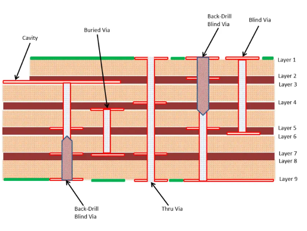
Transitioning to the layout design, the stack-up configuration is a critical aspect.
A well-planned stack-up not only minimizes electromagnetic interference (EMI) but also ensures signal integrity. Typically, a multilayer RF PCB will have dedicated ground and power planes to provide a low-impedance path for return currents, thereby reducing noise and crosstalk. The placement of these planes should be such that they sandwich the signal layers, creating a controlled impedance environment. This is particularly important for high-speed signals, where even minor impedance mismatches can lead to significant signal reflections and losses.
Furthermore, the routing of RF signals demands careful attention.
Microstrip and stripline techniques are commonly employed to route high-frequency signals. Microstrip lines, which are routed on the outer layers, are easier to manufacture but are more susceptible to external noise. On the other hand, stripline routing, which is embedded between two ground planes, offers better noise immunity but is more complex to fabricate. The choice between these techniques depends on the specific requirements of the application, including the operating frequency and the acceptable levels of noise and interference.
In addition to routing techniques, the length and width of the traces must be precisely controlled.
The trace width is determined by the desired characteristic impedance, which is typically 50 ohms for RF applications. Any deviation from this impedance can result in signal reflections, leading to loss of signal integrity. Moreover, the trace length should be minimized to reduce signal delay and attenuation. When long traces are unavoidable, techniques such as serpentine routing can be employed to match the electrical length without increasing the physical length.
Another crucial consideration is the placement of components.
RF components, such as amplifiers, filters, and antennas, should be strategically placed to minimize signal path lengths and avoid interference. Components that are sensitive to noise should be isolated from noisy elements, and proper grounding techniques should be employed to provide a stable reference plane. Additionally, the use of via stitching around critical areas can help in reducing EMI and improving signal integrity.
Thermal management is another vital aspect that cannot be overlooked.
High-frequency operation often results in significant heat generation, which can affect the performance and reliability of the PCB. Effective thermal management strategies, such as the use of thermal vias, heat sinks, and proper airflow design, are essential to dissipate heat efficiently.
Lastly, manufacturability considerations must be integrated into the design process.
The complexity of multilayer RF PCBs can pose challenges during fabrication and assembly. Therefore, it is essential to collaborate closely with the manufacturer to ensure that the design is not only functional but also feasible to produce. Design for manufacturability (DFM) guidelines should be followed to avoid issues such as misalignment, warping, and defects during the production process.
In conclusion, designing a multilayer RF PCB requires a comprehensive understanding of material properties, stack-up configuration, signal routing, component placement, thermal management, and manufacturability. By carefully considering these factors, designers can create high-performance RF PCBs that meet the stringent demands of modern electronic applications.
Common Challenges In Manufacturing Multilayer RF PCB
Manufacturing multilayer RF PCBs (Radio Frequency Printed Circuit Boards) presents a unique set of challenges that require specialized knowledge and meticulous attention to detail. One of the primary difficulties lies in the precise alignment of multiple layers. As the number of layers increases, so does the complexity of ensuring that each layer is accurately aligned with the others. Misalignment can lead to signal integrity issues, which are particularly problematic in RF applications where even minor discrepancies can significantly impact performance.
Another significant challenge is the selection of appropriate materials.
RF PCBs often require substrates with specific dielectric properties to ensure optimal signal transmission. Traditional materials like FR-4 may not always be suitable due to their higher dielectric losses at RF frequencies. Instead, materials such as Rogers or Teflon are often preferred, but these come with their own set of challenges, including higher costs and more complex handling requirements. The choice of material must balance performance, cost, and manufacturability, making it a critical decision in the design and production process.
Thermal management is also a crucial consideration in the manufacturing of multilayer RF PCBs.
The high-frequency signals generate significant heat, which can affect the performance and reliability of the board. Effective thermal management strategies, such as the use of thermal vias and heat sinks, are essential to dissipate heat efficiently. However, incorporating these features into a multilayer design adds another layer of complexity, requiring careful planning and precise execution.
Signal integrity is another area where multilayer RF PCBs pose challenges.
High-frequency signals are susceptible to various forms of interference, including crosstalk and electromagnetic interference (EMI). To mitigate these issues, designers must employ advanced techniques such as controlled impedance routing and the use of ground planes. However, implementing these techniques in a multilayer design can be intricate, requiring a deep understanding of electromagnetic theory and practical experience in PCB layout.
Furthermore, the manufacturing process itself introduces potential pitfalls.
The lamination process, which involves bonding multiple layers together under heat and pressure, must be carefully controlled to avoid defects such as delamination or voids. These defects can compromise the structural integrity of the PCB and lead to failures in the field. Additionally, the drilling and plating processes must be executed with high precision to ensure reliable electrical connections between layers. Any deviation in these processes can result in open or short circuits, which are particularly detrimental in RF applications.
Testing and quality assurance are also more complex for multilayer RF PCBs.
Traditional testing methods may not be sufficient to identify all potential issues, necessitating the use of advanced techniques such as time-domain reflectometry (TDR) and network analyzers. These tools can provide detailed insights into the performance of the PCB, but they also require specialized knowledge to interpret the results accurately.
In conclusion, the manufacturing of multilayer RF PCBs involves a series of intricate challenges that span from material selection and thermal management to signal integrity and precise manufacturing processes. Each step requires careful consideration and expertise to ensure that the final product meets the stringent performance requirements of RF applications. By understanding and addressing these challenges, manufacturers can produce high-quality multilayer RF PCBs that deliver reliable performance in demanding environments.
Applications Of Multilayer RF PCB In Telecommunications
Multilayer RF PCBs, or Radio Frequency Printed Circuit Boards, have become indispensable in the telecommunications industry due to their ability to handle high-frequency signals with minimal interference. These advanced circuit boards are designed to support the complex requirements of modern communication systems, making them a critical component in various applications within the telecommunications sector.
One of the primary applications of multilayer RF PCBs in telecommunications is in the development of mobile communication devices.
As smartphones and other mobile devices continue to evolve, the demand for faster data transmission and improved signal quality has increased. Multilayer RF PCBs are essential in meeting these demands, as they provide the necessary infrastructure to support high-speed data transfer and reliable signal integrity. By incorporating multiple layers of conductive material, these PCBs can efficiently manage the intricate circuitry required for advanced mobile communication technologies such as 4G and 5G networks.
In addition to mobile devices, multilayer RF PCBs play a crucial role in the infrastructure that supports telecommunications networks.
Base stations, which are the backbone of cellular networks, rely on these advanced circuit boards to process and transmit high-frequency signals. The ability of multilayer RF PCBs to minimize signal loss and interference is particularly important in this context, as it ensures that communication between base stations and mobile devices remains clear and uninterrupted. Furthermore, the compact design of multilayer RF PCBs allows for the integration of more components within a smaller footprint, which is essential for the efficient operation of base stations in densely populated urban areas.
Another significant application of multilayer RF PCBs in telecommunications is in satellite communication systems.
Satellites are responsible for transmitting signals over long distances, and the performance of these systems is heavily dependent on the quality of the RF PCBs used. Multilayer RF PCBs are designed to withstand the harsh conditions of space, including extreme temperatures and radiation, while maintaining optimal signal integrity. This makes them ideal for use in satellite communication systems, where reliability and performance are paramount.
Moreover, multilayer RF PCBs are also utilized in the development of advanced radar systems
which are essential for various telecommunications applications, including air traffic control and weather monitoring. These systems require precise signal processing capabilities to accurately detect and track objects, and multilayer RF PCBs provide the necessary infrastructure to achieve this. The ability of these PCBs to handle high-frequency signals with minimal distortion ensures that radar systems can operate effectively and provide accurate data.
Furthermore, the advent of the Internet of Things (IoT) has expanded the scope of telecommunications,
with an increasing number of devices requiring seamless connectivity. Multilayer RF PCBs are integral to the development of IoT devices, as they enable efficient communication between interconnected devices. The compact and efficient design of these PCBs allows for the integration of multiple functionalities within a single device, facilitating the development of sophisticated IoT solutions.
In conclusion, multilayer RF PCBs are a cornerstone of modern telecommunications, enabling the development and operation of a wide range of communication systems. From mobile devices and base stations to satellite communication and radar systems, these advanced circuit boards provide the necessary infrastructure to support high-frequency signal transmission with minimal interference. As the telecommunications industry continues to evolve, the importance of multilayer RF PCBs will only grow, driving innovation and enhancing connectivity across the globe.


