Multilayer rf pcb design
Understanding The Basics Of Multilayer RF PCB Design
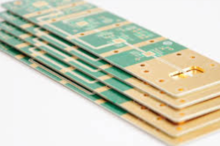
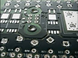
Multilayer RF PCB design is a sophisticated and intricate process that requires a deep understanding of both the theoretical and practical aspects of radio frequency (RF) engineering and printed circuit board (PCB) fabrication.
At its core, a multilayer RF PCB is a complex structure composed of multiple layers of conductive and insulating materials, meticulously arranged to achieve optimal performance in high-frequency applications. The design process begins with a thorough comprehension of the fundamental principles of RF behavior, including signal propagation, impedance control, and electromagnetic interference (EMI) management.
One of the primary considerations in multilayer RF PCB design is the selection of appropriate materials.
The dielectric constant and loss tangent of the substrate materials play a crucial role in determining the signal integrity and overall performance of the PCB. High-frequency signals are particularly sensitive to variations in these parameters, making it essential to choose materials that offer low dielectric loss and stable dielectric properties over a wide frequency range. Additionally, the thermal and mechanical properties of the materials must be compatible with the intended operating environment to ensure long-term reliability.
Another critical aspect of multilayer RF PCB design is the stack-up configuration.
The arrangement of the various layers, including signal, ground, and power planes, must be carefully planned to minimize crosstalk, reduce EMI, and maintain consistent impedance. A well-designed stack-up not only enhances signal integrity but also simplifies the routing of high-frequency signals by providing clear and direct paths. The use of ground planes, in particular, is essential for creating a low-impedance return path for RF signals, thereby reducing the potential for signal degradation and noise coupling.
Transitioning from material selection and stack-up configuration, the next step involves meticulous attention to trace layout and routing.
The width, spacing, and length of traces must be precisely controlled to maintain the desired impedance and minimize signal reflections. Differential pairs, commonly used in high-speed digital and RF designs, require careful matching of trace lengths to ensure signal synchronization. Additionally, the use of via structures, which connect different layers of the PCB, must be optimized to minimize parasitic inductance and capacitance that can adversely affect high-frequency performance.
Furthermore, the integration of passive components, such as resistors, capacitors, and inductors, into the multilayer RF PCB design demands careful consideration.
These components must be strategically placed to achieve the desired filtering, matching, and decoupling functions without introducing unwanted parasitic effects. Surface-mount technology (SMT) components are often preferred for their compact size and superior high-frequency performance compared to through-hole components.
As the design progresses, simulation and modeling become indispensable tools for validating the performance of the multilayer RF PCB.
Electromagnetic simulation software allows designers to predict the behavior of RF signals within the PCB, identify potential issues, and make necessary adjustments before physical prototyping. This iterative process helps to refine the design, ensuring that it meets the stringent requirements of high-frequency applications.
Finally, the manufacturing process itself must be carefully managed to preserve the integrity of the multilayer RF PCB design.
Precision in fabrication, including accurate layer alignment, controlled etching, and consistent lamination, is essential to achieve the desired electrical performance. Post-fabrication testing, including impedance measurements and signal integrity analysis, provides a final verification of the design’s compliance with specifications.
In conclusion, understanding the basics of multilayer RF PCB design involves a comprehensive approach that encompasses material selection, stack-up configuration, trace layout, component integration, simulation, and precise manufacturing. Each step is interdependent, requiring careful consideration and expertise to ensure the successful implementation of high-performance RF circuits.
Key Considerations For Signal Integrity In Multilayer RF PCBs
When designing multilayer RF PCBs, ensuring signal integrity is paramount. Signal integrity refers to the quality and reliability of the electrical signals as they travel through the PCB. In RF applications, where high-frequency signals are prevalent, maintaining signal integrity becomes even more critical due to the susceptibility of these signals to various forms of interference and degradation. Several key considerations must be taken into account to preserve signal integrity in multilayer RF PCB designs.
Firstly, the choice of materials plays a crucial role.
The dielectric material used in the PCB substrate must have low dielectric loss and stable dielectric constant over the operating frequency range. Materials such as Rogers or Teflon are often preferred for RF applications due to their superior electrical properties compared to standard FR-4. These materials help minimize signal loss and ensure consistent signal propagation, which is essential for maintaining signal integrity.
Another important consideration is the stack-up configuration of the multilayer PCB.
The stack-up determines the arrangement of signal and ground layers, which directly impacts the impedance control and electromagnetic compatibility (EMC) of the design. A well-planned stack-up can help reduce crosstalk and electromagnetic interference (EMI) by providing adequate isolation between signal layers and incorporating ground planes. Ground planes act as reference planes for signal traces, helping to maintain a consistent impedance and reduce noise.
Impedance control is another critical aspect of signal integrity in RF PCB design.
Impedance mismatches can cause signal reflections, leading to signal degradation and loss. To achieve proper impedance control, designers must carefully calculate the trace widths, spacing, and the distance between signal traces and reference planes. Tools such as impedance calculators and simulation software can aid in this process, ensuring that the impedance of the signal traces matches the characteristic impedance of the transmission lines.
Furthermore, the routing of signal traces must be meticulously planned.
High-frequency signals are particularly sensitive to trace length, bends, and vias. To minimize signal degradation, traces should be kept as short and straight as possible. When bends are necessary, they should be gradual rather than sharp to avoid impedance discontinuities. Additionally, the use of vias should be minimized, as they can introduce inductance and capacitance that affect signal integrity. When vias are unavoidable, techniques such as back-drilling can be employed to remove the unused portion of the via, thereby reducing its impact on the signal.
Power integrity is also a vital consideration in multilayer RF PCB design.
Stable and clean power delivery is essential for maintaining signal integrity. Decoupling capacitors should be strategically placed close to the power pins of active components to filter out noise and provide a stable power supply. The power distribution network (PDN) should be designed to minimize voltage drops and noise, ensuring that all components receive a consistent and clean power supply.
Lastly, thermal management should not be overlooked.
High-frequency components can generate significant heat, which can affect their performance and, consequently, the signal integrity. Proper thermal management techniques, such as the use of thermal vias, heat sinks, and adequate ventilation, should be implemented to dissipate heat effectively and maintain the reliability of the PCB.
In conclusion, maintaining signal integrity in multilayer RF PCB designs requires careful consideration of material selection, stack-up configuration, impedance control, trace routing, power integrity, and thermal management. By addressing these key factors, designers can ensure that their RF PCBs deliver reliable and high-quality performance, even in demanding high-frequency applications.
Advanced Techniques For Minimizing Crosstalk In Multilayer RF PCB Design
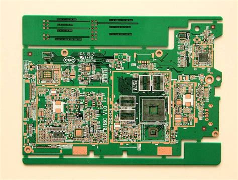
In the realm of multilayer RF PCB design, minimizing crosstalk is a critical challenge that demands advanced techniques and meticulous attention to detail. Crosstalk, the unwanted coupling of signals between adjacent traces, can significantly degrade the performance of RF circuits, leading to signal integrity issues and reduced overall system reliability. To address this, designers must employ a combination of strategic layout practices, careful material selection, and sophisticated simulation tools.
One of the fundamental strategies for minimizing crosstalk in multilayer RF PCB design is the thoughtful arrangement of signal layers and ground planes.
By placing ground planes adjacent to signal layers, designers can create a shielding effect that helps to contain electromagnetic fields and reduce the potential for crosstalk. Additionally, maintaining a consistent and minimal spacing between signal traces and their corresponding ground planes can further enhance this shielding effect, thereby improving signal integrity.
Another crucial technique involves the use of differential signaling, which can significantly mitigate crosstalk.
Differential pairs, consisting of two complementary signals, are designed to carry equal and opposite currents. This configuration not only enhances noise immunity but also reduces the electromagnetic interference (EMI) that can lead to crosstalk. By ensuring that differential pairs are tightly coupled and maintaining consistent spacing between them, designers can effectively minimize the impact of crosstalk on signal quality.
Moreover, the careful routing of signal traces plays a pivotal role in crosstalk reduction.
Designers should aim to route high-speed and high-frequency signals on separate layers from low-speed and low-frequency signals. This segregation helps to prevent the coupling of high-frequency noise into sensitive low-frequency circuits. Additionally, avoiding parallel routing of signal traces over long distances can significantly reduce the likelihood of crosstalk. When parallel routing is unavoidable, increasing the spacing between traces can help to mitigate the effects of crosstalk.
The selection of appropriate PCB materials is another critical factor in minimizing crosstalk.
High-frequency laminates with low dielectric constants and low loss tangents are preferred for RF PCB designs, as they exhibit lower signal attenuation and reduced crosstalk. Furthermore, the use of materials with high thermal stability can help to maintain consistent electrical properties, thereby ensuring reliable performance over a wide range of operating conditions.
Advanced simulation tools also play an indispensable role in the design process, enabling designers to predict and analyze crosstalk before the physical PCB is fabricated.
Electromagnetic simulation software can model the behavior of signals within the PCB, allowing designers to identify potential sources of crosstalk and optimize the layout accordingly. By iterating through multiple design scenarios and evaluating their impact on crosstalk, designers can arrive at an optimal solution that balances performance, manufacturability, and cost.
In addition to these techniques, implementing proper decoupling and filtering strategies can further enhance crosstalk mitigation.
Placing decoupling capacitors close to power supply pins and using ferrite beads to filter high-frequency noise can help to maintain a clean power supply, thereby reducing the potential for crosstalk. Additionally, incorporating ground vias and stitching vias can improve the grounding system, providing a low-impedance path for return currents and further minimizing crosstalk.
In conclusion, minimizing crosstalk in multilayer RF PCB design requires a multifaceted approach that encompasses strategic layout practices, careful material selection, and the use of advanced simulation tools. By employing these advanced techniques, designers can achieve superior signal integrity, enhance system reliability, and ensure optimal performance in high-frequency applications.
Material Selection And Its Impact On Multilayer RF PCB Performance
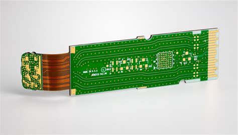
Material selection plays a pivotal role in the performance of multilayer RF PCB designs. The choice of materials directly influences the electrical, thermal, and mechanical properties of the final product, thereby affecting its overall functionality and reliability. To begin with, the dielectric constant (Dk) of the substrate material is a critical parameter. A consistent and low Dk is essential for maintaining signal integrity and minimizing signal loss. Materials such as PTFE (Polytetrafluoroethylene) and ceramic-filled laminates are often preferred due to their stable dielectric properties over a wide frequency range.
In addition to the dielectric constant, the dissipation factor (Df) is another crucial consideration.
A low Df indicates minimal energy loss as the signal propagates through the PCB, which is particularly important for high-frequency applications. Materials with low dissipation factors, such as Rogers RO3000 series, are commonly used in RF PCB designs to ensure efficient signal transmission.
Thermal management is another aspect significantly impacted by material selection.
High-frequency circuits generate substantial heat, which can degrade performance and reduce the lifespan of the PCB. Therefore, materials with high thermal conductivity are essential to dissipate heat effectively. For instance, ceramic-filled PTFE composites not only offer excellent electrical properties but also provide superior thermal management, making them ideal for high-power RF applications.
Mechanical stability is equally important in multilayer RF PCB design.
The materials must withstand various environmental stresses, including temperature fluctuations, humidity, and mechanical vibrations. Materials like FR-4, although widely used in general PCB applications, may not always meet the stringent requirements of RF designs. Instead, high-performance materials such as hydrocarbon ceramic laminates are often chosen for their robustness and reliability under harsh conditions.
Furthermore, the coefficient of thermal expansion (CTE) of the materials must be compatible with the components mounted on the PCB.
A mismatch in CTE can lead to mechanical stresses during thermal cycling, potentially causing delamination or solder joint failures. Materials with a low and matched CTE, such as certain ceramic-filled substrates, help mitigate these risks, ensuring long-term reliability.
The choice of materials also affects the manufacturability of the multilayer RF PCB.
Some high-performance materials may pose challenges during fabrication, such as difficulties in drilling or etching. Therefore, it is essential to balance performance requirements with manufacturability to achieve a cost-effective and reliable design. Collaborating closely with material suppliers and PCB manufacturers can help in selecting materials that meet both performance and production criteria.
Moreover, the surface finish of the PCB is influenced by the material selection.
Surface finishes like ENIG (Electroless Nickel Immersion Gold) or immersion silver are often used in RF PCBs to ensure good solderability and low contact resistance. The compatibility of these finishes with the chosen substrate material must be considered to avoid issues such as oxidation or poor adhesion.
In conclusion, material selection is a multifaceted decision that significantly impacts the performance of multilayer RF PCB designs. By carefully considering factors such as dielectric properties, thermal management, mechanical stability, and manufacturability, designers can optimize their PCBs for high-frequency applications. The collaboration between designers, material suppliers, and manufacturers is crucial in navigating the complexities of material selection, ultimately leading to the successful implementation of high-performance RF PCBs.

