New technology in pcb manufacturing
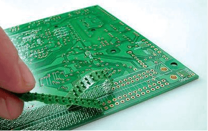
Advances In Flexible PCB Technology
Flexible printed circuit boards (PCBs) have revolutionized the electronics industry, offering a myriad of advantages over traditional rigid PCBs. As technology continues to advance, the development of flexible PCBs has seen significant progress, driven by the demand for more compact, lightweight, and versatile electronic devices.
One of the most notable advancements in flexible PCB technology is the improvement in materials used for their construction.
Polyimide and polyester substrates have become the materials of choice due to their excellent thermal stability, mechanical flexibility, and electrical insulation properties. These materials enable the creation of PCBs that can bend, twist, and fold without compromising their functionality, making them ideal for applications in wearable electronics, medical devices, and aerospace technology.
In addition to material advancements, the manufacturing processes for flexible PCBs have also seen significant improvements.
Traditional photolithography techniques have been enhanced with the introduction of laser direct imaging (LDI) technology. LDI allows for higher precision and accuracy in the creation of circuit patterns, resulting in finer lines and spaces, which are essential for the miniaturization of electronic components. This technology not only improves the overall quality of flexible PCBs but also reduces production time and costs, making it more accessible for various industries.
Moreover, the integration of advanced surface mount technology (SMT) has further propelled the capabilities of flexible PCBs.
SMT allows for the placement of smaller and more complex components onto the flexible substrate, enhancing the functionality and performance of the final product. This is particularly beneficial for the development of high-density interconnect (HDI) flexible PCBs, which are essential for modern electronic devices that require high-speed data transmission and increased signal integrity.
Another significant advancement in flexible PCB technology is the development of stretchable PCBs.
Unlike traditional flexible PCBs that can only bend and fold, stretchable PCBs can expand and contract, providing even greater design flexibility. This innovation is particularly valuable in the field of wearable electronics, where devices must conform to the contours of the human body while maintaining their functionality. Stretchable PCBs are made possible through the use of novel materials such as conductive inks and elastomeric substrates, which can withstand repeated stretching and bending without losing their electrical properties.
Furthermore, the advent of additive manufacturing, commonly known as 3D printing, has opened new possibilities for flexible PCB production.
3D printing allows for the creation of complex, multi-layered circuit structures with precise control over the placement of conductive and insulating materials. This technology enables the production of customized flexible PCBs with unique shapes and configurations, catering to specific application requirements. Additionally, 3D printing reduces material waste and production costs, making it an environmentally friendly and cost-effective solution for flexible PCB manufacturing.
In conclusion, the advancements in flexible PCB technology have significantly expanded the potential applications of electronic devices.
The improvements in materials, manufacturing processes, and integration techniques have resulted in more reliable, efficient, and versatile flexible PCBs. As technology continues to evolve, it is expected that flexible PCBs will play an increasingly important role in the development of next-generation electronic devices, driving innovation across various industries. The ongoing research and development in this field promise to bring even more exciting advancements, further pushing the boundaries of what is possible with flexible PCB technology.
Innovations In PCB Miniaturization
The field of printed circuit board (PCB) manufacturing has witnessed significant advancements over the past few decades, with miniaturization emerging as a pivotal innovation. This trend towards smaller, more efficient PCBs is driven by the increasing demand for compact electronic devices, such as smartphones, wearables, and medical implants. As a result, manufacturers are continually exploring new technologies to meet these evolving requirements.
One of the most notable innovations in PCB miniaturization is the development of high-density interconnect (HDI) technology.
HDI PCBs are characterized by their finer lines and spaces, smaller vias, and higher connection pad density. This technology allows for more components to be placed on a smaller board, thereby reducing the overall size of the device. Moreover, HDI technology enhances signal integrity and performance, which is crucial for high-speed applications. The use of microvias, which are significantly smaller than traditional vias, is a key feature of HDI PCBs. These microvias enable the creation of multi-layer boards with complex interconnections, further contributing to the miniaturization of electronic devices.
In addition to HDI technology, the advent of flexible PCBs has also played a significant role in the miniaturization of electronic devices.
Flexible PCBs, made from materials such as polyimide or polyester, can be bent, folded, and twisted without damaging the circuitry. This flexibility allows for more innovative and compact designs, particularly in applications where space is limited. For instance, flexible PCBs are commonly used in wearable technology, where they can conform to the shape of the human body. Furthermore, the integration of rigid-flex PCBs, which combine the benefits of both rigid and flexible boards, has opened up new possibilities for miniaturization. These hybrid boards provide the mechanical stability of rigid PCBs while offering the design flexibility of flexible PCBs.
Another groundbreaking innovation in PCB miniaturization is the use of advanced materials and fabrication techniques.
For example, the incorporation of low-loss materials, such as liquid crystal polymer (LCP) and polytetrafluoroethylene (PTFE), has improved the performance of high-frequency circuits. These materials exhibit excellent electrical properties, such as low dielectric constant and low dissipation factor, which are essential for maintaining signal integrity in miniaturized PCBs. Additionally, advancements in photolithography and laser drilling techniques have enabled the production of finer features and more precise interconnections. These techniques allow for the creation of smaller components and tighter tolerances, which are critical for achieving higher levels of miniaturization.
Moreover, the integration of embedded components within the PCB substrate has emerged as a promising approach to miniaturization.
By embedding passive components, such as resistors and capacitors, within the layers of the PCB, manufacturers can save valuable surface space and reduce the overall size of the board. This approach also improves the reliability and performance of the circuit by minimizing parasitic effects and reducing the length of interconnections. The use of embedded components is particularly advantageous in applications where space constraints are a primary concern, such as in medical devices and aerospace electronics.
In conclusion, the continuous advancements in PCB manufacturing technologies have significantly contributed to the miniaturization of electronic devices. Innovations such as HDI technology, flexible and rigid-flex PCBs, advanced materials, and embedded components have enabled manufacturers to create smaller, more efficient, and higher-performing PCBs. As the demand for compact electronic devices continues to grow, it is expected that further developments in PCB miniaturization will continue to shape the future of the electronics industry.

The Role Of AI In PCB Design And Manufacturing
The integration of artificial intelligence (AI) into printed circuit board (PCB) design and manufacturing is revolutionizing the industry, offering unprecedented levels of efficiency, precision, and innovation. As the demand for more complex and compact electronic devices grows, traditional methods of PCB design and manufacturing are increasingly being supplemented, and in some cases replaced, by AI-driven technologies. This transformation is not only enhancing the capabilities of engineers and manufacturers but also significantly reducing the time and cost associated with PCB production.
One of the primary ways AI is impacting PCB design is through the automation of the design process.
Traditionally, PCB design has been a labor-intensive task requiring meticulous attention to detail. Engineers had to manually place components and route connections, a process that could take days or even weeks for complex boards. However, AI algorithms can now analyze design requirements and automatically generate optimized layouts in a fraction of the time. These algorithms consider various factors such as signal integrity, power distribution, and thermal management, ensuring that the final design meets all necessary specifications. Consequently, engineers can focus more on innovation and less on repetitive tasks, leading to faster development cycles and quicker time-to-market for new products.
In addition to automating design, AI is also enhancing the accuracy and reliability of PCB manufacturing.
Machine learning models can predict potential manufacturing defects by analyzing vast amounts of data from previous production runs. By identifying patterns and correlations that might be missed by human inspectors, these models can flag issues before they occur, allowing for preemptive adjustments to the manufacturing process. This predictive capability not only reduces the incidence of defects but also minimizes waste and rework, contributing to more sustainable manufacturing practices.
Moreover, AI-driven quality control systems are becoming increasingly sophisticated.
Vision systems equipped with AI can inspect PCBs at various stages of production, identifying defects such as misaligned components, soldering issues, and surface imperfections with high precision. These systems can operate continuously and at high speeds, far surpassing the capabilities of manual inspection. As a result, manufacturers can ensure higher quality standards and reduce the likelihood of faulty products reaching the market.
Another significant advantage of AI in PCB manufacturing is its ability to facilitate real-time monitoring and optimization of production processes.
By integrating AI with the Internet of Things (IoT) devices, manufacturers can collect and analyze data from various stages of the production line. This real-time data analysis enables dynamic adjustments to be made, optimizing parameters such as temperature, pressure, and assembly speed to maintain optimal production conditions. Consequently, manufacturers can achieve higher yields and more consistent product quality.
Furthermore, AI is playing a crucial role in supply chain management for PCB manufacturing.
Predictive analytics can forecast demand for components and materials, allowing manufacturers to manage inventory more effectively and avoid shortages or overstock situations. This capability is particularly valuable in an industry where supply chain disruptions can have significant impacts on production schedules and costs.
In conclusion, the role of AI in PCB design and manufacturing is multifaceted and transformative. By automating design processes, enhancing manufacturing accuracy, improving quality control, optimizing production, and streamlining supply chain management, AI is driving significant advancements in the industry. As AI technologies continue to evolve, their integration into PCB manufacturing will undoubtedly lead to even greater efficiencies and innovations, shaping the future of electronics in ways that were previously unimaginable.
Eco-Friendly Materials In PCB Production
The evolution of printed circuit board (PCB) manufacturing has seen significant advancements over the years, with a growing emphasis on sustainability and environmental responsibility. As the demand for electronic devices continues to surge, the industry faces increasing pressure to adopt eco-friendly materials and processes. This shift towards greener practices is not only driven by regulatory requirements but also by a collective commitment to reducing the environmental footprint of electronic products.
One of the most notable developments in eco-friendly PCB production is the introduction of biodegradable substrates.
Traditional PCBs are typically made from fiberglass and epoxy resins, which are not biodegradable and pose significant disposal challenges. In contrast, biodegradable substrates, such as those made from natural fibers and bio-based resins, offer a sustainable alternative. These materials decompose more easily, reducing the long-term environmental impact of discarded electronic devices. Moreover, they can be sourced from renewable resources, further enhancing their eco-friendly credentials.
In addition to biodegradable substrates, the industry is also exploring the use of non-toxic, lead-free soldering materials.
Lead-based solders have been a staple in PCB manufacturing for decades due to their reliability and low cost. However, lead is a hazardous material that poses serious health and environmental risks. The transition to lead-free solders, such as those made from tin-silver-copper alloys, represents a significant step towards safer and more sustainable PCB production. These alternatives not only meet stringent environmental regulations but also offer comparable performance characteristics, ensuring that the quality and reliability of electronic devices are maintained.
Another promising development in eco-friendly PCB manufacturing is the adoption of water-based fluxes and cleaning agents.
Traditional fluxes and cleaning solvents often contain volatile organic compounds (VOCs) and other harmful chemicals that can contribute to air and water pollution. Water-based alternatives, on the other hand, are less toxic and produce fewer emissions, making them a more environmentally friendly choice. Additionally, these water-based solutions can be more easily recycled and treated, further minimizing their environmental impact.
The push for sustainability in PCB production also extends to energy consumption.
Manufacturing processes can be energy-intensive, contributing to greenhouse gas emissions and resource depletion. To address this, many companies are investing in energy-efficient equipment and practices. For instance, the use of advanced manufacturing technologies, such as laser drilling and direct imaging, can reduce energy consumption and material waste. Furthermore, the implementation of renewable energy sources, such as solar and wind power, in manufacturing facilities can significantly lower the carbon footprint of PCB production.
Recycling and reusing materials is another critical aspect of eco-friendly PCB manufacturing.
The recovery of valuable metals, such as gold, silver, and copper, from discarded PCBs not only conserves natural resources but also reduces the need for mining and refining activities, which are often environmentally damaging. Innovative recycling techniques, such as hydrometallurgical and biotechnological processes, are being developed to efficiently extract these metals while minimizing environmental harm.
In conclusion, the shift towards eco-friendly materials and practices in PCB manufacturing is a multifaceted effort that encompasses biodegradable substrates, lead-free solders, water-based fluxes, energy-efficient technologies, and advanced recycling methods. As the industry continues to innovate and adopt sustainable solutions, it is poised to significantly reduce its environmental impact while meeting the growing demand for electronic devices. This commitment to sustainability not only benefits the planet but also aligns with the evolving expectations of consumers and regulatory bodies, ensuring a greener future for PCB manufacturing.


