New Technology in PCB Manufacturing: Revolutionizing the Electronics Industry
Introduction
The Printed Circuit Board (PCB) is the backbone of modern electronics, serving as the foundation for virtually every electronic device, from smartphones and computers to medical equipment and automotive systems. As the demand for smaller, faster, and more efficient electronic devices continues to grow, the PCB manufacturing industry is undergoing a significant transformation. New technologies are emerging that are revolutionizing the way PCBs are designed, fabricated, and assembled. These advancements are not only improving the performance and reliability of PCBs but also enabling the development of next-generation electronics that were previously unimaginable.
This article explores the latest technological innovations in PCB manufacturing, including advancements in materials, fabrication techniques, design tools, and assembly processes. We will also discuss the implications of these technologies for the electronics industry and the challenges that lie ahead.
1. Advanced Materials for PCBs
One of the most significant areas of innovation in PCB manufacturing is the development of new materials. Traditional PCBs are typically made from fiberglass-reinforced epoxy resin (FR-4), which has been the industry standard for decades. However, as electronic devices become more complex and operate at higher frequencies, the limitations of FR-4 are becoming increasingly apparent. New materials are being developed to address these challenges and enable the production of PCBs with superior performance characteristics.
a. High-Frequency Laminates
With the advent of 5G technology and the increasing demand for high-speed data transmission, there is a growing need for PCBs that can operate at higher frequencies. High-frequency laminates, such as Rogers, Taconic, and Isola materials, are designed to minimize signal loss and maintain signal integrity at frequencies above 1 GHz. These materials have lower dielectric constants and dissipation factors compared to traditional FR-4, making them ideal for high-frequency applications.
b. Flexible and Stretchable Substrates
Flexible and stretchable PCBs are becoming increasingly important in applications such as wearable electronics, medical devices, and flexible displays. These PCBs are made from materials such as polyimide (PI) and liquid crystal polymer (LCP), which offer excellent flexibility, thermal stability, and chemical resistance. In addition, stretchable substrates made from elastomers and conductive inks are being developed for applications that require the PCB to conform to irregular shapes or withstand mechanical deformation.
c. Thermally Conductive Materials
As electronic devices become more powerful, managing heat dissipation is becoming a critical challenge. Traditional PCBs are not well-suited for high-power applications due to their limited thermal conductivity. New materials, such as metal-core PCBs (MCPCBs) and thermally conductive laminates, are being developed to improve heat dissipation and prevent overheating. These materials typically incorporate a metal layer, such as aluminum or copper, which acts as a heat sink to dissipate heat away from critical components.
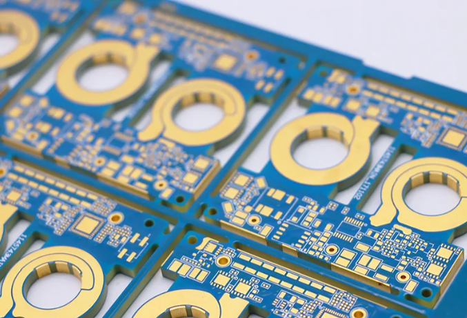
2. Advanced Fabrication Techniques
In addition to new materials, advancements in fabrication techniques are also driving innovation in PCB manufacturing. These techniques are enabling the production of PCBs with higher precision, greater complexity, and improved performance.
a. Additive Manufacturing (3D Printing)
Additive manufacturing, or 3D printing, is revolutionizing the way PCBs are fabricated. Traditional PCB manufacturing involves subtractive processes, such as etching and drilling, which can be time-consuming and generate significant waste. In contrast, 3D printing allows for the direct deposition of conductive and insulating materials, enabling the rapid prototyping and production of complex PCB designs.
One of the most promising applications of 3D printing in PCB manufacturing is the production of multi-layer PCBs with embedded components. By depositing conductive traces and insulating layers layer by layer, 3D printing can create PCBs with integrated passive components, such as resistors and capacitors, as well as active components, such as transistors and diodes. This approach not only reduces the size and weight of the PCB but also improves its electrical performance by minimizing parasitic inductance and capacitance.
b. Laser Direct Imaging (LDI)
Laser Direct Imaging (LDI) is an advanced photolithography technique that is replacing traditional UV exposure methods in PCB manufacturing. LDI uses a laser to directly expose the photoresist on the PCB, eliminating the need for a photomask. This allows for higher resolution and greater precision in the patterning of conductive traces, enabling the production of PCBs with finer features and tighter tolerances.
LDI is particularly well-suited for high-density interconnect (HDI) PCBs, which are used in applications such as smartphones, tablets, and other compact electronic devices. HDI PCBs require extremely fine traces and small vias, which can be challenging to achieve with traditional photolithography methods. LDI enables the production of HDI PCBs with trace widths and spacings as small as 25 microns, as well as microvias with diameters of less than 50 microns.
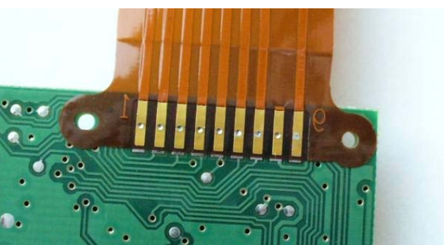
c. Embedded Components
Embedding components within the PCB substrate is another emerging trend in PCB manufacturing. This technique involves placing passive components, such as resistors, capacitors, and inductors, directly into the layers of the PCB, rather than mounting them on the surface. Embedded components offer several advantages, including reduced PCB size, improved electrical performance, and enhanced reliability.
Embedded components are particularly beneficial for high-frequency and high-speed applications, where minimizing parasitic effects is critical. By embedding components within the PCB, the length of the interconnects is reduced, which in turn reduces signal loss and improves signal integrity. In addition, embedded components are less susceptible to mechanical stress and thermal cycling, making them more reliable in harsh environments.
3. Advanced Design Tools and Simulation Software
The complexity of modern PCBs is increasing, driven by the demand for higher performance, smaller form factors, and greater functionality. To meet these challenges, PCB designers are turning to advanced design tools and simulation software that enable them to create more sophisticated and optimized designs.
a. High-Speed Design Tools
High-speed design tools are essential for designing PCBs that can operate at high frequencies and data rates. These tools allow designers to analyze signal integrity, power integrity, and electromagnetic compatibility (EMC) during the design phase, rather than after the PCB has been fabricated. By simulating the behavior of signals and power distribution networks, designers can identify and mitigate potential issues before they become problems.
One of the key features of high-speed design tools is the ability to perform time-domain and frequency-domain analysis. Time-domain analysis allows designers to evaluate the transient behavior of signals, such as rise time, fall time, and overshoot, while frequency-domain analysis enables them to assess the frequency response of the PCB, including impedance matching and resonance.
b. Multi-Physics Simulation
Multi-physics simulation software is becoming increasingly important in PCB design, particularly for applications that involve thermal management, mechanical stress, and fluid dynamics. These tools allow designers to simulate the interaction between different physical phenomena, such as heat transfer, mechanical deformation, and fluid flow, within the PCB.
For example, multi-physics simulation can be used to optimize the thermal performance of a PCB by modeling the heat generated by components and the heat dissipation through the PCB substrate and surrounding environment. This allows designers to identify hot spots and implement cooling solutions, such as heat sinks or thermal vias, to prevent overheating.
c. Artificial Intelligence (AI) and Machine Learning (ML)
Artificial intelligence (AI) and machine learning (ML) are beginning to play a role in PCB design and manufacturing. AI-powered design tools can analyze large datasets of PCB designs and manufacturing processes to identify patterns and optimize designs for performance, cost, and manufacturability. ML algorithms can also be used to predict potential defects and failures during the manufacturing process, enabling proactive quality control.
In addition, AI and ML are being used to automate the PCB design process, reducing the time and effort required to create complex designs. For example, AI-powered routing algorithms can automatically generate optimal trace layouts, taking into account factors such as signal integrity, power distribution, and thermal management.
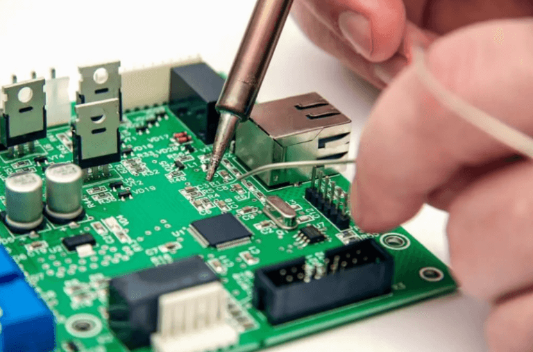
4. Advanced Assembly Techniques
The assembly of PCBs is also benefiting from new technologies that are improving the accuracy, efficiency, and reliability of the process. These advancements are enabling the production of PCBs with higher component densities and more complex interconnects.
a. Surface Mount Technology (SMT)
Surface Mount Technology (SMT) has been the dominant method for assembling PCBs for several decades, and it continues to evolve with new advancements. SMT involves mounting components directly onto the surface of the PCB, rather than inserting them through holes. This allows for higher component densities and more compact designs.
Recent advancements in SMT include the development of smaller and more precise pick-and-place machines, which can handle components with sizes as small as 01005 (0.4 mm x 0.2 mm). In addition, new solder paste formulations and reflow soldering techniques are improving the reliability of SMT assemblies, particularly for fine-pitch components and high-density interconnects.
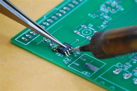
b. Chip-on-Board (CoB) and Chip-on-Flex (CoF)
Chip-on-Board (CoB) and Chip-on-Flex (CoF) are advanced assembly techniques that involve mounting bare semiconductor chips directly onto the PCB or flexible substrate, rather than using packaged components. This approach eliminates the need for traditional packaging, reducing the size and weight of the PCB and improving electrical performance.
CoB and CoF are particularly well-suited for applications that require high component densities and compact form factors, such as wearable electronics, medical devices, and IoT sensors. In addition, these techniques offer improved thermal performance, as the bare chips can be directly bonded to the PCB or substrate, allowing for more efficient heat dissipation.
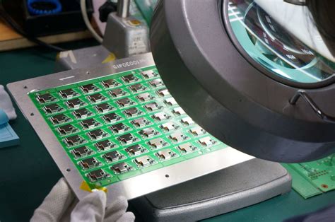
c. Automated Optical Inspection (AOI) and X-Ray Inspection
As PCBs become more complex and component densities increase, the need for reliable inspection methods is becoming more critical. Automated Optical Inspection (AOI) and X-Ray Inspection are advanced techniques that are being used to detect defects and ensure the quality of PCB assemblies.
AOI uses high-resolution cameras and image processing algorithms to inspect the surface of the PCB for defects such as missing components, misaligned components, and solder bridges. X-Ray Inspection, on the other hand, allows for the inspection of hidden features, such as solder joints under Ball Grid Array (BGA) components and vias within the PCB layers.
These inspection techniques are essential for ensuring the reliability of high-density and high-complexity PCBs, particularly in applications where failure is not an option, such as aerospace, medical, and automotive electronics.
5. Implications for the Electronics Industry
The advancements in PCB manufacturing technology are having a profound impact on the electronics industry. These innovations are enabling the development of smaller, faster, and more efficient electronic devices, as well as new applications that were previously not possible.
a. Miniaturization and Increased Functionality
One of the most significant implications of new PCB technologies is the continued trend toward miniaturization and increased functionality. As PCBs become smaller and more complex, electronic devices can be made more compact and lightweight, while still offering advanced features and capabilities. This is particularly important for applications such as smartphones, wearables, and IoT devices, where size and weight are critical factors.
b. Improved Performance and Reliability
The use of advanced materials, fabrication techniques, and design tools is also improving the performance and reliability of PCBs. High-frequency laminates, embedded components, and advanced assembly techniques are enabling the production of PCBs that can operate at higher speeds and frequencies, with lower signal loss and improved thermal management. This is essential for applications such as 5G communications, autonomous vehicles, and high-performance computing.
c. New Applications and Markets
The advancements in PCB manufacturing are also opening up new applications and markets. For example, flexible and stretchable PCBs are enabling the development of wearable electronics, medical devices, and flexible displays. Similarly, 3D-printed PCBs are being used in rapid prototyping and custom electronics, where traditional manufacturing methods are not feasible.
6. Challenges and Future Directions
While the new technologies in PCB manufacturing offer significant benefits, they also present several challenges that need to be addressed. These challenges include the high cost of advanced materials and equipment, the need for specialized skills and expertise, and the potential environmental impact of new manufacturing processes.
a. Cost and Accessibility
One of the main challenges of adopting new PCB technologies is the high cost of advanced materials, equipment, and processes. For example, high-frequency laminates and 3D printing systems can be significantly more expensive than traditional materials and methods. This can make it difficult for smaller companies and startups to adopt these technologies, limiting their accessibility.
b. Skills and Expertise
The complexity of new PCB technologies also requires specialized skills and expertise, both in design and manufacturing. Designers need to be familiar with advanced design tools and simulation software, while manufacturers need to have the knowledge and experience to work with new materials and processes. This can create a skills gap that needs to be addressed through education and training.
c. Environmental Impact
Finally, the environmental impact of new PCB manufacturing technologies is a growing concern. The use of advanced materials, such as high-frequency laminates and flexible substrates, can generate more waste and require more energy to produce. In addition, the disposal of electronic waste (e-waste) is becoming a significant issue, particularly as electronic devices become more complex and difficult to recycle.
To address these challenges, the PCB industry is exploring more sustainable materials and manufacturing processes, as well as developing recycling and reuse programs for electronic components and materials.
Conclusion
The PCB manufacturing industry is undergoing a period of rapid innovation, driven by the demand for smaller, faster, and more efficient electronic devices. New materials, fabrication techniques, design tools, and assembly processes are revolutionizing the way PCBs are designed, fabricated, and assembled, enabling the development of next-generation electronics that were previously unimaginable.
While these advancements offer significant benefits, they also present challenges that need to be addressed, including cost, accessibility, skills, and environmental impact. As the industry continues to evolve, it will be essential to strike a balance between innovation and sustainability, ensuring that the benefits of new technologies are realized while minimizing their impact on the environment and society.
In the coming years, we can expect to see even more exciting developments in PCB manufacturing, as new materials, processes, and technologies continue to push the boundaries of what is possible in electronics. The future of PCB manufacturing is bright, and the possibilities are endless.