New Technology in PCB Manufacturing: Revolutionizing the Electronics Industry
Introduction
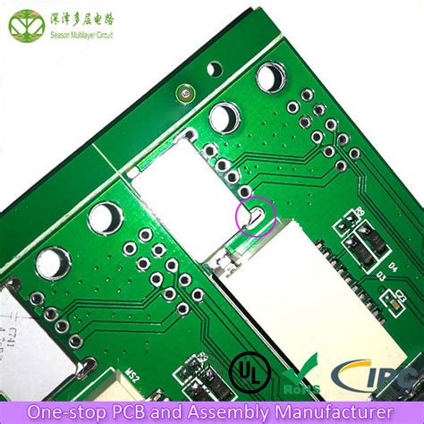
The Printed Circuit Board (PCB) is the backbone of modern electronics, serving as the foundation for virtually every electronic device we use today. From smartphones and laptops to medical devices and automotive systems, PCBs are integral to the functionality and performance of these technologies. As the demand for smaller, faster, and more efficient electronic devices continues to grow, the PCB manufacturing industry has been forced to innovate and adopt new technologies to meet these evolving needs. This article explores the latest advancements in PCB manufacturing, highlighting how these innovations are revolutionizing the electronics industry.
1. Advanced Materials for Enhanced Performance
One of the most significant advancements in PCB manufacturing is the development and adoption of advanced materials. Traditional PCBs are typically made from FR-4, a glass-reinforced epoxy laminate material. While FR-4 has been the industry standard for decades, it has limitations in terms of thermal performance, signal integrity, and mechanical strength, especially in high-frequency and high-power applications.
To address these limitations, manufacturers are now turning to alternative materials such as:
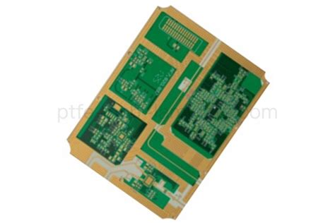
- High-Frequency Laminates: These materials, such as Rogers, Taconic, and PTFE (Polytetrafluoroethylene), offer superior electrical properties, including low dielectric loss and stable dielectric constants, making them ideal for high-frequency applications like 5G communications and radar systems.
- Metal Core PCBs (MCPCBs): MCPCBs use a metal base, typically aluminum or copper, to provide better thermal conductivity. This is particularly useful in LED lighting, power electronics, and automotive applications where heat dissipation is critical.
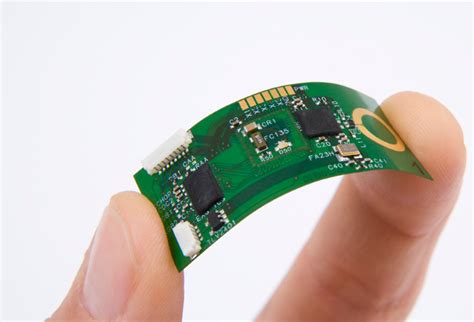
- Flexible and Rigid-Flex PCBs: These PCBs use flexible materials like polyimide to create boards that can bend and fold, enabling more compact and lightweight designs. Rigid-flex PCBs combine the benefits of both rigid and flexible boards, offering greater design flexibility and reliability in complex applications.
2. Additive Manufacturing and 3D Printing
Additive manufacturing, commonly known as 3D printing, is making waves in the PCB industry. Traditional PCB manufacturing involves subtractive processes, where copper is etched away from a substrate to create the desired circuit pattern. In contrast, additive manufacturing builds the PCB layer by layer, allowing for more complex and precise designs.
- Direct Ink Writing (DIW): DIW is a 3D printing technique that uses conductive inks to print circuit traces directly onto a substrate. This method eliminates the need for etching and allows for the creation of intricate, multi-layered circuits with minimal waste.
- Aerosol Jet Printing: This advanced 3D printing technology uses a fine mist of conductive ink to print circuits with high precision. Aerosol jet printing is particularly useful for creating fine-pitch traces and embedding components directly into the PCB.
- 3D Printed Electronics: Beyond just printing circuits, 3D printing is being used to create entire electronic devices with integrated PCBs. This approach enables the production of highly customized and compact devices, reducing the need for assembly and streamlining the manufacturing process.
3. Embedded Components and System-in-Package (SiP) Technology
As electronic devices become smaller and more complex, the demand for higher component density on PCBs has increased. Embedded component technology addresses this challenge by integrating passive components (resistors, capacitors, and inductors) directly into the PCB substrate. This not only saves space but also improves electrical performance by reducing parasitic effects and signal loss.
- Embedded Active Components: In addition to passive components, manufacturers are now embedding active components, such as ICs, directly into the PCB. This approach, known as System-in-Package (SiP) technology, allows for the creation of highly integrated and compact electronic systems.
- Fan-Out Wafer-Level Packaging (FOWLP): FOWLP is an advanced packaging technology that redistributes the I/O connections of a chip across a larger area, allowing for higher pin counts and better thermal performance. This technology is particularly useful in mobile devices and IoT applications where space is at a premium.
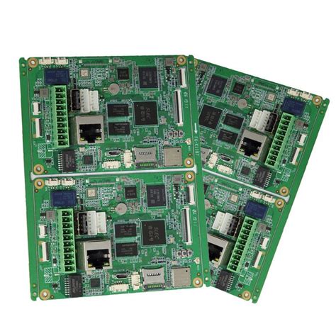
4. High-Density Interconnect (HDI) Technology
High-Density Interconnect (HDI) technology is another game-changer in PCB manufacturing. HDI PCBs feature finer lines and spaces, smaller vias, and higher connection pad density, enabling the creation of more compact and complex circuits. This technology is essential for modern electronics, where the demand for miniaturization and high performance is ever-increasing.
- Microvias: HDI PCBs use microvias, which are small laser-drilled holes that connect different layers of the board. Microvias allow for higher routing density and improved signal integrity, making them ideal for high-speed and high-frequency applications.
- Sequential Lamination: HDI PCBs often require multiple lamination cycles to build up the layers of the board. Sequential lamination allows for the creation of complex multi-layer structures with precise control over the thickness and alignment of each layer.
- Any-Layer HDI: Any-layer HDI takes the concept of microvias to the next level by allowing vias to be placed on any layer of the PCB. This provides even greater design flexibility and enables the creation of ultra-compact and high-performance PCBs.
5. Automation and Industry 4.0 in PCB Manufacturing
The fourth industrial revolution, or Industry 4.0, is transforming PCB manufacturing through the integration of automation, data exchange, and smart technologies. Automation is becoming increasingly prevalent in PCB production, from automated optical inspection (AOI) to robotic assembly and testing.
- Automated Optical Inspection (AOI): AOI systems use high-resolution cameras and advanced algorithms to inspect PCBs for defects such as solder bridges, missing components, and misaligned traces. AOI improves quality control and reduces the risk of defects in the final product.
- Robotic Assembly: Robots are being used to place and solder components onto PCBs with high precision and speed. Robotic assembly not only increases production efficiency but also reduces the risk of human error.
- Smart Factories: Industry 4.0 is driving the adoption of smart factories, where machines and systems are interconnected and can communicate with each other in real-time. This enables predictive maintenance, real-time monitoring, and data-driven decision-making, leading to higher productivity and lower costs.
6. Environmental Sustainability in PCB Manufacturing
As the electronics industry continues to grow, so does its environmental impact. PCB manufacturing traditionally involves the use of hazardous chemicals, generates significant waste, and consumes large amounts of energy. However, new technologies are emerging to make PCB production more sustainable.
- Lead-Free Soldering: The transition to lead-free soldering has been a major step towards reducing the environmental impact of PCB manufacturing. Lead-free solder alloys, such as SAC (Tin-Silver-Copper), are now widely used, reducing the release of toxic lead into the environment.
- Green PCB Materials: Manufacturers are increasingly using eco-friendly materials, such as halogen-free laminates and recyclable substrates, to reduce the environmental footprint of PCBs.
- Waste Reduction and Recycling: Advanced manufacturing techniques, such as additive manufacturing, generate less waste compared to traditional subtractive methods. Additionally, recycling programs for PCBs and electronic waste are becoming more widespread, helping to recover valuable materials and reduce landfill.
7. The Role of Artificial Intelligence (AI) and Machine Learning (ML)
Artificial Intelligence (AI) and Machine Learning (ML) are playing an increasingly important role in PCB manufacturing. These technologies are being used to optimize production processes, improve quality control, and enhance design capabilities.
- Predictive Maintenance: AI algorithms can analyze data from manufacturing equipment to predict when maintenance is needed, reducing downtime and preventing costly breakdowns.
- Quality Control: Machine learning models can be trained to identify defects in PCBs with high accuracy, improving the efficiency of quality control processes.
- Design Optimization: AI-powered design tools can analyze and optimize PCB layouts for performance, manufacturability, and cost. These tools can suggest improvements to the design, such as reducing signal interference or optimizing component placement.
Conclusion
The PCB manufacturing industry is undergoing a period of rapid transformation, driven by the need for smaller, faster, and more efficient electronic devices. Advanced materials, additive manufacturing, embedded components, HDI technology, automation, sustainability, and AI are just some of the innovations that are reshaping the industry. These new technologies are not only improving the performance and reliability of PCBs but also enabling the creation of more complex and compact electronic systems.
As the demand for electronics continues to grow, the PCB manufacturing industry will need to continue innovating to meet the challenges of the future. By embracing these new technologies, manufacturers can stay ahead of the curve and continue to drive the evolution of the electronics industry. The future of PCB manufacturing is bright, and the possibilities are endless.