Notes on PCB design of audio interface circuit
Audio interface is an audio jack, that is, an audio interface, which can be divided into Audio in interface and Audio out interface. Audio interface is a device that connects microphones and other sound sources to computers, and it plays a role of bridging the connection between analog and digital signals.
The other routing requirements are as follows:
- It is recommended to connect 22ohm resistors in series to all CLK signals and place them close to RK3588 to improve signal quality;
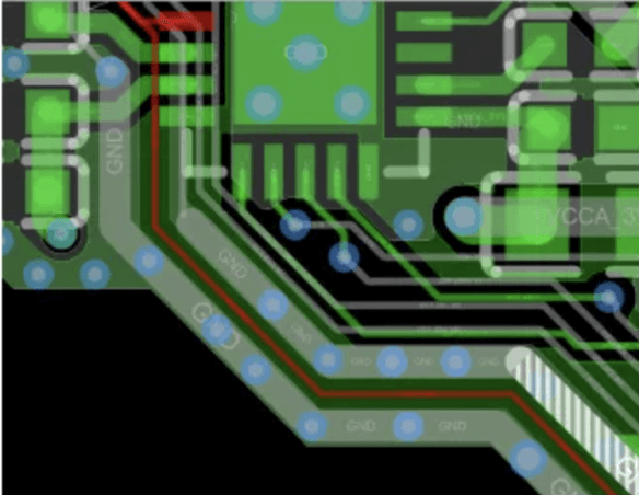
- All CLK signal routing must not be close together to avoid crosstalk; the clock signal needs to be independently wrapped throughout the whole process, and a ground via must be drilled within 300mil of the wiring interval of the wrapped ground; as shown in Figure 1
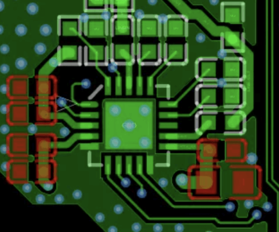
- The decoupling capacitors of each IO power supply of the chip must be placed close to the chip; as shown in Figure 2.
- The audio interface is placed according to the structure. If there is no structural requirement, it should be placed on the edge of the board as much as possible for easy plugging and unplugging;
- The IC is placed close to the interface, not too far away, and the analog signal is as short as possible.
- Audio in and Audio out do not need to control impedance, the routing needs to be thickened to 15mil, the whole process is grounded, and a ground via must be drilled every 300mil;
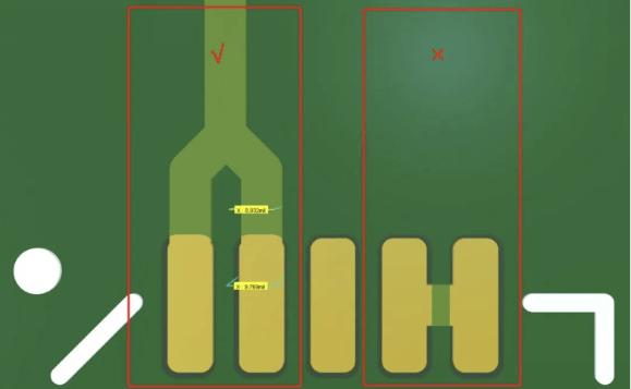
- ESD devices should be placed close to the audio interface. The routing needs to warn the ESD device when entering the audio interface, and do not punch holes to change layers, as shown in
- All audio signal lines should be routed away from the inductor area, away from RF signals and devices;
- For an I2S interface connected to multiple devices, the related CLKs should be connected according to the daisy chain routing topology; for a PDM interface connected to multiple devices, the related CLKs should be connected according to the daisy chain routing topology; if GPIO is sufficient, both CLKs in a group of PDM interfaces can be used to optimize routing branches;
- All audio signals should be away from high-speed signal lines such as LCD and DRAM. It is forbidden to route on the adjacent layer of the high-speed signal line. The adjacent layer of the audio signal must be the ground plane. It is forbidden to punch holes and change layers near the high-speed signal line;
- It is recommended to wrap the SPDIF signal with ground throughout, and the wiring interval of the ground is 300mil There must be a ground via within;
For the requirements of peripheral audio signals, please refer to the corresponding device design guide. If there is no emphasis, please refer to the following instructions:
- The SPKP/SPKN signal coupling routing of the speaker is carried out, and the whole group is wrapped with ground. The line width is calculated according to the peak current of the output, and the routing is shortened as much as possible to control the line resistance;
- If the amplifier output of the speaker is placed with magnetic beads, LC filters and other devices, it is recommended to place them close to the amplifier output to optimize EMI;
- The left and right channel outputs of the Headphone should be wrapped with ground independently to avoid crosstalk and optimize isolation. The recommended routing width is greater than 10mil;
- When the microphone is connected single-ended, the MIC signal is routed separately and wrapped with ground separately; when the microphone is connected differentially, especially in most pseudo-differential cases, it is also necessary to follow the differential routing and wrap the whole group with ground;
- The routing width of the microphone signal is recommended to be 8mil Above;
- For the TVS protection diodes of the headphone jack and microphone, place them as close to the connector as possible, and the signal topology is: headphone jack/microphone→TVS→IC; in this way, when ESD occurs, the ESD current will first pass through the TVS device to attenuate; there should be no residual piles on the TVS device routing, and it is recommended to increase the ground vias of the TVS ground pin as much as possible, and at least ensure two 0.4mm*0.2mm vias to enhance the electrostatic discharge capability.