Offline Switching Power Supply (SMPS) Design Solution
Offline switching power supply (SMPS) is a classic product that converts grid power to DC power according to the terminal load. Usually, this switching power supply contains two conversion stages, and in order to achieve higher efficiency, it is necessary to use better power switches or implement different control strategies. In addition, it is also important to choose a more suitable topology according to the specific situation. This system solution guide will introduce the basics about offline SMPS, as well as selected products and solutions from ON Semiconductor. This article is the first part, and it will focus on system usage, system implementation, system description, market information and trends.
Offline switching power supply (SMPS) is a classic product that converts grid power to DC power according to the terminal load. Usually, this switching power supply contains two conversion stages, and in order to achieve higher efficiency, it is necessary to use better power switches or implement different control strategies. In addition, it is also important to choose a more suitable topology according to the specific situation. This system solution guide will introduce the basics about offline SMPS, as well as selected products and solutions from ON Semiconductor. This article is the first part, and it will focus on system usage, system implementation, system description, market information and trends.
System Purpose
Since the last century, offline SMPS has been attracting much attention, with related research emerging one after another and being widely used in all aspects of daily life. Offline SMPS generally refers to a switching power supply with an isolation transformer and powered by the power grid. Its application range ranges from 65W laptop battery chargers to multi-kilowatt data center server power supply units.
Wide bandgap semiconductor products are emerging in an endless stream, allowing manufacturers to adopt new topologies to optimize efficiency, size and integration levels according to actual conditions. Newly designed controllers can also help improve system safety, reduce power consumption and improve performance.
In order to achieve the global “zero carbon” goal, SMPS must meet stricter efficiency standards to minimize energy consumption and carbon emissions. For example, in order to promote energy conservation and emission reduction, the newly released CoC V5 of the European Commission and the DoE VI of the US Department of Energy have clear requirements for power loss and efficiency at full load and light load/no load.
System Implementation
Power engineers must read, offline switching power supply (SMPS) system design nanny-level tutorial
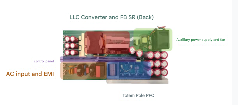
3kw totem pole PFC+LLC PSU reference design
Power engineers must read, offline switching power supply (SMPS) system design nanny-level tutorial
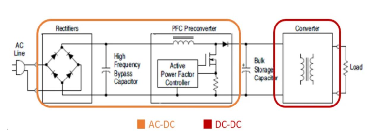
Typical offline SMPS
System Description
- Standards
There are currently three main types of standards, including safety standards and radiation standards. The latest revised IEC 62368-1 second edition belongs to the safety standard, which clarifies the definitions of concepts such as insulation, isolation, electrical clearance, and creepage distance. IEC 61000-3-2 is an international radiation standard that limits power supply voltage distortion by specifying the maximum value of harmonic currents from the 2nd harmonic to the 40th harmonic. This standard applies to devices with a rated current not exceeding 16A, and devices with a rated current greater than 16A should follow IEC 61000-3-12.
To promote energy conservation and emission reduction, relevant regulations and standards have been formulated around the world, such as those formulated by the California Energy Commission, Energy Star certification, and the European Union’s Energy-Related Products (ErP) Directive. The U.S. Department of Energy (DoE) has issued a set of classification standards for wall-mounted or desktop external power supplies, of which Level VI is the latest and most stringent standard; at the same time, the European Commission’s scientific and knowledge service agency “Joint Research Center” has developed a set of EU External Power Supply (EPS) Code of Conduct (CoC).
In addition, there is the 80 PLUS® program, which is committed to promoting 80% or higher efficiency at 20% to 100% load conditions and 0.9 or higher power factor at 100% load conditions. Its highest level (i.e., the “80+ Titanium” standard) stipulates that the efficiency must be at least 92% at 20% load and at least 94% at 100% load.
- Power Factor Correction
PFC (power factor correction) is a key component of offline power supplies. The main tasks of PFC are to shape the input current and reduce high-frequency harmonic currents. The former can increase the actual power obtained from the main power supply, while the latter can reduce the losses and costs associated with distribution, generation and important equipment in the process. THD (Total Harmonic Distortion) is an important method to determine the quality of line current in the system and is often used as a substitute for power factor. Another important value of the PFC stage is that it can provide a stable DC output voltage, which can provide a narrow range of DC input for the subsequent isolated DC-DC converter, thereby optimizing the overall design.
- DC-DC stage
The role of the DC-DC stage is to convert a certain range of input voltages to the required DC output voltage and current through an isolation transformer and a PWM or resonant converter. The key challenge of the DC-DC stage lies in the design of magnetic components. For example, skin effect and proximity effect can cause eddy currents in high-frequency transformers, affect the selection of core materials, cause core losses and copper losses, etc.
- Current control mode
It is necessary to review the classic working mode here, because the working mode not only affects the choice of topology, but also affects the design of the entire system. CCM (Continuous Conduction Mode) provides very low peak and rms currents, so it is more used in applications with higher power levels. In CCM, the inductor current ripple is small, but the MOSFET is turned on when the boost diode is conducting. So we need to use a low trr diode to avoid excessive losses and stress when the MOSFET is turned on. CrM (Critical Conduction Mode) is very suitable for low power applications.
In this mode, the inductor current starts the next cycle after reaching zero, and the frequency varies with the line voltage and load conditions. A big advantage of CrM is that the current loop is inherently stable and does not require slope compensation. In addition, the inductor current drops to zero every cycle, so there is no reverse recovery loss in the diode when turning off, and even a cheaper boost diode will not degrade performance. Similarly, the MOSFET can be turned on at a low voltage, thereby reducing switching losses.
Usually when the system is lightly loaded, CrM/CCM switches to DCM (Discontinuous Conduction Mode) to ensure a high power factor and suppress EMI caused by a large increase in frequency near the zero crossing point.
FCCrM (Frequency Clamped Critical Conduction Mode) is a method proposed by ON Semiconductor to limit the switching frequency expansion of CrM circuits. When the converter is running at light load and/or near the line voltage zero crossing point, the maximum frequency clamp forces the system to switch to DCM. If such a circuit is not used, the CrM switching frequency will exceed the clamping upper limit, resulting in increased switching losses. At this time, a circuit must be added to compensate for the dead time generated by DCM to keep the line current in the correct waveform.
- Wide Bandgap Semiconductors
Wide bandgap devices are being mass-produced, and many companies have launched (or are about to launch) SMPS based on SiC/GaN. SiC/GaN materials have many advantages such as excellent reverse recovery performance, excellent thermal performance, high operating voltage and temperature, which can allow new systems to increase frequency and reduce PCB size, and even do not require heat sinks or forced heat dissipation. However, high frequency may bring potential problems such as radiation and overshoot, so we must develop new designs.
- Integration
PCB space can be saved and external passive components can be reduced, which can improve power density and installation flexibility. For example, GaN HEMT is a popular choice for low and medium power supplies (Pout < 1500W), which can significantly reduce the size of the final product. When dv/dt may exceed 100V/ns, we need to reduce parasitic inductance. Integrating GaN HEMT and driver in the same package can reduce the inductance caused by leads and PCB, resulting in better switching performance.
- New topologies can improve efficiency
Totem pole PFC reduces the losses caused by the rectifier bridge, making it a better PFC topology than single boost in high power density products. Today, LLC has become the preferred DC-DC topology for medium and high power applications with a wider soft switching range, a narrow frequency range throughout the load change process, and a small circulating current. Wide bandgap semiconductors play a key role in these new topologies, and intelligent low-power controllers are another important factor for high efficiency.

