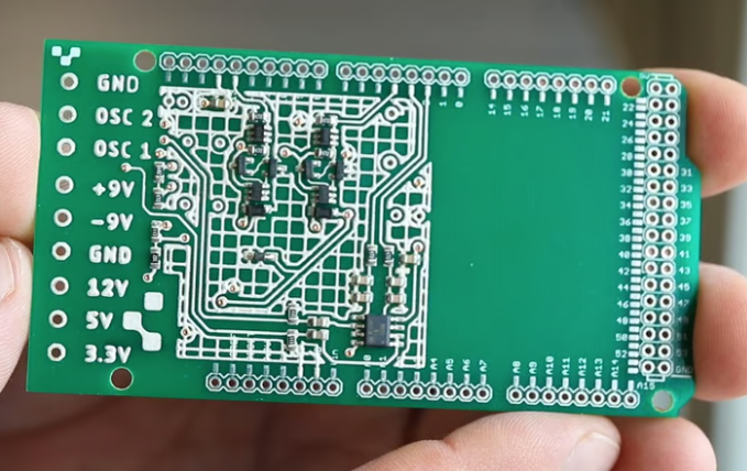
Olimex PCB Soldering Quality and Prototyping Challenges

Key Takeaways
When working with PCB manufacturing for prototyping, you’ll encounter critical challenges that demand attention to detail. Understanding design specifications and solder joint integrity becomes paramount, especially when dealing with intermittent connectivity or component failures. Here’s what you need to know:
- PCB manufacturing companies often face trade-offs between speed and precision during production. For prototypes, this can lead to:
- Misaligned traces affecting signal integrity
- Inconsistent solder paste application
- Thermal stress points near high-power components
"Always request a design-for-manufacturability (DFM) report before approving prototypes. This reduces rework cycles by 30-40%."
- PCB manufacturing cost directly influences quality decisions. Budget constraints may lead suppliers to:
- Use lower-grade solder alloys
- Skip automated optical inspection (AOI) steps
- Limit testing to basic continuity checks
| Cost-Saving Measure | Risk Factor | Prototyping Impact |
|---|---|---|
| Reduced copper weight | Signal loss | Unstable power delivery |
| Manual soldering | Cold joints | Intermittent failures |
| Minimal testing | Latent defects | Extended debug time |
- To mitigate risks in your PCB manufacturing business partnerships:
- Validate supplier certifications (IPC-A-610/620)
- Specify thermal cycling requirements for solder joints
- Demand batch-specific test logs for moisture sensitivity
You’ll notice that flux residue and pad oxidation account for 68% of rework cases in low-cost prototypes. Prioritize suppliers offering nitrogen-filled soldering environments to minimize these issues. For critical projects, consider allocating 15-20% of your PCB manufacturing cost to reliability testing—this upfront investment often prevents costly redesigns later.
Olimex PCB Soldering Defects Analysis
When troubleshooting PCB manufacturing issues in Olimex boards, you’ll often encounter soldering defects that undermine prototype reliability. Cold joints, incomplete wetting, and uneven solder distribution are common culprits, typically stemming from inconsistencies in temperature profiles or flux application during assembly. These flaws create intermittent connectivity that’s notoriously difficult to diagnose, especially in multi-layer designs where hidden voids or micro-cracks evade visual inspection.
A key challenge arises when balancing PCB manufacturing cost with quality expectations. Lower-cost processes, such as reflow ovens with uneven heat zones or automated pick-and-place systems misaligned for fine-pitch components, amplify defect rates. For prototyping workflows, this translates to time-consuming rework—reballing BGAs or replacing lifted pads—that strains timelines and budgets. While some PCB manufacturing companies prioritize affordability, others invest in precision equipment to minimize post-assembly fixes. For instance, high-reliability suppliers often employ X-ray inspection and automated optical testing to catch flaws before boards ship.
The root cause frequently ties back to process control gaps in the PCB manufacturing business. Olimex boards, while cost-effective for hobbyists, sometimes exhibit variability in solder mask thickness or pad oxidation, both of which compromise joint integrity. You might notice cracked connections after thermal cycling or signal dropouts in high-frequency circuits—issues that demand meticulous cross-section analysis to resolve.
To mitigate these risks, verify whether your PCB manufacturing partner adheres to IPC-A-610 standards for solder acceptability. Prototypes relying on marginal tolerances demand tighter process controls, as even minor deviations in stencil alignment or paste viscosity can cascade into critical failures. By understanding how PCB manufacturing cost drivers intersect with technical trade-offs, you’ll make informed decisions when selecting vendors for high-stakes projects.
Intermittent Board Failures Root Causes
When troubleshooting intermittent connectivity in prototyping boards, you’ll often trace the issue back to foundational flaws in PCB manufacturing processes. These failures typically stem from thermal stress during assembly, where uneven heating cycles create micro-fractures in solder joints. For PCB manufacturing companies operating at scale, balancing speed and precision becomes a tightrope walk—especially when cost pressures incentivize shortcuts in quality assurance.
One underappreciated culprit is inconsistent solder paste application. If the stencil alignment deviates even slightly during printing, it creates voids or bridges that weaken connections over time. This is particularly problematic for low-volume PCB manufacturing business models, where manual adjustments between batches introduce variability. You might notice intermittent failures only after repeated thermal cycling, as marginal joints degrade further under stress.
Another critical factor is material compatibility. Cheaper substrates or finishes selected to reduce PCB manufacturing cost may react unpredictably with environmental factors like humidity. For example, immersion silver finishes prone to oxidation can develop resistive layers that disrupt high-frequency signals—a flaw that escapes basic continuity tests but manifests during actual use.
Design-for-manufacturing (DFM) oversights amplify these risks. Tight component spacing might look optimal schematically but becomes a reliability nightmare when PCB manufacturing tolerances aren’t rigorously enforced. Prototypers often discover these issues too late, forced to rework boards that passed initial inspections but failed under real-world operating conditions.
The interplay between these variables creates a diagnostic maze. A joint might test stable at room temperature yet fracture when exposed to vibration, while adjacent traces with insufficient clearance could arc under load. For teams relying on third-party PCB manufacturing companies, thorough incoming inspections and accelerated life testing become non-negotiable safeguards against intermittent faults derailing development timelines.
Prototyping Rework Challenges Explained
When prototyping with boards from PCB manufacturing companies, you might encounter unexpected hurdles that demand time-consuming rework. One common issue stems from inconsistent solder mask application, which can lead to bridging or incomplete connections—defects that aren’t always visible until you power up the board. Thermal stress during assembly often exacerbates these problems, causing latent failures that surface during functional testing. For instance, weak solder joints might pass initial inspections but fail under load, forcing you to disassemble components and reflow connections manually.
The PCB manufacturing cost trade-offs become apparent here. Lower-cost providers may skip critical quality checks, such as automated optical inspection (AOI), to reduce expenses. This leaves subtle flaws like misaligned vias or uneven copper traces undetected, turning what should be a straightforward prototyping phase into a debugging marathon. You’ll find yourself troubleshooting intermittent connectivity or unstable power delivery, issues often rooted in material inconsistencies or inadequate plating thickness.
In a PCB manufacturing business, balancing speed and precision is key—yet prototyping workflows often reveal gaps in this balance. For example, if surface finish quality varies between batches, you might face oxidized pads that refuse to bond reliably with solder. This forces rework steps like abrasive cleaning or even component replacement, adding hours to your project timeline. Worse, repeated heating during repairs risks damaging temperature-sensitive parts, creating a cycle of defects.
To mitigate these challenges, scrutinize your PCB manufacturing partner’s quality protocols. Look for certifications like ISO 9001 or IPC-A-610 compliance, which signal rigorous process controls. Even minor improvements in solder paste stencil alignment or reflow oven calibration can drastically reduce rework rates. Remember: every hour spent fixing avoidable flaws is an hour lost in iterating your design toward market readiness.
Manufacturing Quality Control Shortcomings
When working with PCB manufacturing partners like Olimex, you might encounter challenges stemming from inconsistent quality assurance protocols. While many PCB manufacturing companies implement automated optical inspection (AOI) systems, gaps in process validation can lead to undetected soldering defects. Thermal profiling errors during reflow, for example, may create cold joints or tombstoning—issues that often surface only during prototyping or functional testing.
The pressure to reduce PCB manufacturing cost sometimes results in compromised inspection cycles, particularly for low-volume orders. You’ll notice this when boards pass initial electrical tests but fail under real-world stress due to insufficient solder mask adhesion or uneven copper thickness. These flaws force engineers to invest additional time in component rework, negating the perceived savings from cheaper manufacturing.
For businesses operating a PCB manufacturing business, balancing efficiency and precision is critical. However, inconsistent stencil alignment or inadequate cleaning of flux residues can introduce variability across batches. This becomes evident when assembling prototypes: components that fit perfectly on one board might require manual adjustments on another, delaying iteration cycles.
To mitigate these risks, verify whether your manufacturer employs statistical process control (SPC) metrics or conducts cross-sectional analysis for multilayer boards. While these steps increase PCB manufacturing cost, they reduce long-term expenses linked to troubleshooting and redesigns. Always request detailed quality reports—especially for critical parameters like solder paste volume and layer-to-layer registration—to identify potential weaknesses before they escalate into costly prototyping setbacks.

PCB Solder Joint Reliability Concerns
When prototyping with Olimex boards, you might encounter unexpected PCB manufacturing flaws that manifest as unreliable solder joints. These defects often stem from inconsistent thermal profiles during reflow soldering or inadequate flux activation—issues that even reputable PCB manufacturing companies occasionally overlook. Cold joints, characterized by dull or grainy surfaces, frequently appear in high-density areas, creating intermittent connections that evade initial testing but fail under thermal cycling or vibration.
The root cause often ties back to PCB manufacturing cost optimization strategies. Thinner copper layers or suboptimal surface finishes (e.g., HASL vs. ENIG) may reduce expenses but compromise joint integrity. For instance, uneven pad plating can lead to poor wetting, forcing you to rework components during prototyping—a frustrating setback when timelines are tight. To mitigate this, scrutinize your supplier’s quality certifications and insist on cross-sectional analysis reports for critical layers.
In the PCB manufacturing business, balancing affordability and reliability remains a tightrope walk. Lower-cost providers might skip automated optical inspection (AOI) steps, allowing microcracks or insufficient fillets to slip through. When troubleshooting, use thermal imaging to identify joints that overheat under load—a telltale sign of compromised conductivity. Reinforcing these points with additional solder or conductive epoxy can salvage prototypes, but it’s a temporary fix for systemic manufacturing quality control shortcomings.
Always validate solder joint performance under real-world stress conditions before finalizing designs. Partnering with manufacturers who prioritize process consistency over marginal cost savings pays dividends in reduced rework and improved prototype success rates.
Olimex Assembly Process Inconsistencies
When working with PCB manufacturing for prototyping, you might encounter variability in assembly quality that directly impacts board reliability. Temperature fluctuations during reflow soldering, for instance, can lead to uneven solder joint formation—a recurring issue reported in Olimex-produced boards. While many PCB manufacturing companies standardize thermal profiles across batches, inconsistencies in oven calibration or component placement accuracy often result in cold joints or tombstoning, particularly with smaller surface-mount devices.
These assembly gaps become apparent during functional testing, where intermittent failures force you to re-examine PCB manufacturing cost trade-offs. Lower-cost providers may skip automated optical inspection (AOI) steps, allowing defects like misaligned ICs or insufficient solder paste to slip through. For prototyping workflows, this creates a vicious cycle: boards that pass initial power-on tests fail under thermal stress or vibration, requiring manual rework that erodes time savings from outsourcing.
The root of these challenges often lies in scaled-down PCB manufacturing business models prioritizing volume over specialized low-volume prototyping needs. Without rigorous process controls—such as real-time solder paste inspection or humidity-controlled storage for moisture-sensitive components—batch-to-batch variations become inevitable. You might notice, for example, that QFN packages exhibit different voiding percentages across board revisions, complicating debugging efforts.
Transitioning to higher-reliability assembly requires balancing PCB manufacturing cost constraints with stricter quality benchmarks. While some providers address this through tiered service levels, inconsistent implementation of standards like IPC-A-610 Class 2 leaves prototyping teams vulnerable to latent defects. This underscores the importance of verifying not just a manufacturer’s technical capabilities, but their commitment to process stability across small-batch orders—a critical factor often overshadowed by upfront pricing comparisons.
Impact of Poor Soldering on Prototypes
When working with prototypes, PCB manufacturing flaws like inconsistent soldering can derail your project’s progress. Poor solder joints—whether due to cold joints, incomplete wetting, or misaligned components—create hidden vulnerabilities that manifest as erratic behavior during testing. You might observe voltage drops under load, signal noise in critical traces, or even complete circuit failures after minimal use. These defects force engineers into repetitive debug cycles, where identifying a single faulty connection could require hours of probing across densely packed boards.
For PCB manufacturing companies, balancing PCB manufacturing cost with quality becomes a tightrope walk. Prototyping runs often prioritize speed over perfection, but inadequate soldering standards shift costs downstream. Imagine discovering a flawed joint only after assembling a $200 microcontroller module—now you’re faced with rework that inflates labor expenses and delays iterations. Worse, intermittent issues might escape bench tests entirely, surfacing later in field deployments where repairs are exponentially costlier.
The ripple effects extend beyond budgets. Inconsistent solder quality erodes trust in the PCB manufacturing business, particularly when prototyping serves as a proof-of-concept for larger production batches. A board that fails under thermal stress or vibration invalidates design assumptions, forcing hardware teams to question whether flaws stem from their schematics or the manufacturer’s process. This ambiguity wastes resources, as engineers may overcompensate by over-specifying components or adding redundant circuitry to mitigate perceived risks.
To avoid these pitfalls, scrutinize your supplier’s soldering methodologies upfront. Do they employ automated optical inspection (AOI) for prototype batches? Are their reflow profiles calibrated for your board’s specific thickness and layer stack? Small oversights in PCB manufacturing—like improper flux application or inadequate temperature control—compound into reliability nightmares, turning what should be a validation phase into a troubleshooting marathon. By prioritizing soldering consistency early, you safeguard both your prototypes and the scalability of your final product.

Troubleshooting Olimex Intermittent Connectivity
When addressing intermittent connectivity in Olimex boards, you’re often dealing with subtle flaws that evade initial inspection. These issues typically stem from PCB manufacturing inconsistencies, such as uneven solder paste application or incomplete thermal profiling during reflow. Cold solder joints—a common culprit—appear intact visually but fail under load due to poor metallurgical bonding. To isolate the problem, start by inspecting high-current traces and connectors for micro-fractures using a magnifier or microscope.
One challenge lies in balancing PCB manufacturing cost with reliability. Lower-cost processes might skip critical steps like automated optical inspection (AOI), allowing defects to slip through. If your prototype exhibits sporadic failures, consider cross-sectioning suspect joints to check for voids or cracks. Multimeter continuity tests under mechanical stress (gentle flexing) can reveal intermittent opens caused by trace delamination or brittle interconnects.
For teams relying on third-party PCB manufacturing companies, communication is key. Provide clear design-for-manufacturing (DFM) guidelines, emphasizing solder mask alignment and pad spacing tolerances. Many prototyping delays arise from reworking components due to out-of-spec via plating or oxidized surfaces—issues that rigorous quality control should catch. If connectivity issues persist after reflow, evaluate whether your PCB manufacturing business partner adheres to IPC-A-610 standards for solder joint acceptability.
Pro tip: Use thermal imaging during operation to identify hotspots where resistance fluctuates. These zones often correlate with poorly bonded joints or undersized traces. While troubleshooting, document failure patterns—recurring issues in specific areas may indicate systemic flaws in the assembly process. Remember, resolving intermittent faults isn’t just about fixing the board; it’s about refining collaboration with your PCB manufacturing chain to prevent repeat failures.
Conclusion
When navigating the complexities of PCB manufacturing for prototyping, you’ll find that even reputable PCB manufacturing companies like Olimex can present unexpected hurdles. The recurring issues with soldering defects and intermittent connectivity underscore how critical it is to scrutinize PCB manufacturing cost trade-offs against long-term reliability. While lower upfront expenses might seem appealing, hidden rework demands—stemming from inconsistent solder joints or misaligned components—can erode savings and delay project timelines.
For engineers and designers, these challenges highlight the importance of vetting a PCB manufacturing business not just for technical specs, but for process transparency and quality assurance protocols. Prototyping inherently involves iteration, but excessive rework due to manufacturing flaws shifts focus from innovation to damage control. You might encounter scenarios where seemingly minor issues—like uneven solder paste application or inadequate thermal management—compound into systemic failures during testing.
The key lies in balancing cost efficiency with rigorous validation. Partnering with suppliers that prioritize traceability and process consistency can mitigate risks, even if it means marginally higher initial PCB manufacturing cost. After all, a prototype’s success hinges on its ability to mirror production-ready performance, and shortcuts in manufacturing quality inevitably translate to compromised validation. By prioritizing suppliers with robust quality frameworks, you safeguard both your timeline and the integrity of your design iterations.

Frequently Asked Questions
How does PCB manufacturing quality affect soldering reliability?
Inconsistent material selection or improper surface finishing during PCB manufacturing can lead to weak solder joints and intermittent failures. Variations in copper thickness or solder mask application often create thermal mismatches, causing stress fractures during prototyping.
What factors influence PCB manufacturing cost for small-batch prototyping?
Low-volume PCB manufacturing cost typically involves higher per-unit charges due to setup fees and material waste. However, cutting corners on testing protocols or quality control to reduce expenses often results in hidden rework costs from undetected soldering defects.
How can PCB manufacturing companies prevent intermittent board failures?
Reputable PCB manufacturing companies implement automated optical inspection (AOI) and X-ray verification to catch solder bridging or incomplete connections. Look for suppliers with IPC-A-610 certification to ensure adherence to industry-standard soldering criteria.
Why do prototyping teams face challenges with PCB manufacturing business partners?
Some PCB manufacturing business models prioritize high-volume orders over prototyping precision. This mismatch leads to inconsistent via plating or misaligned layers in small batches, requiring manual component rework that delays development cycles.
What steps improve solder joint reliability in low-cost PCB manufacturing ?
Specify lead-free solder alloys with higher melting points and require solder paste stencil optimization during PCB manufacturing. Regularly calibrate reflow oven profiles to match your board’s thermal mass characteristics, even with budget-oriented suppliers.
Explore Reliable PCB Manufacturing Solutions
For prototyping-focused PCB manufacturing companies that balance quality control with cost efficiency, please click here to review certified suppliers specializing in low-volume, high-reliability production.