One-Stop Online PCB Design & Manufacturing Solutions
Key Takeaways
When exploring PCB manufacturing solutions, you need platforms that merge professional design support with industrial-grade production capabilities. Leading PCB manufacturing companies now offer end-to-end digital interfaces that let you upload schematics, simulate layouts, and receive instant quotes—all within a single dashboard. This eliminates back-and-forth communications, accelerating timelines for both prototyping and full-scale production.
A critical advantage lies in real-time component pricing visibility. Advanced platforms integrate global supplier databases, allowing you to compare PCB manufacturing cost variables like material grades, layer counts, and surface finishes. For example, opting for FR-4 over high-frequency laminates could reduce expenses by 30–60% in bulk orders, while still meeting technical specifications.
For complex projects, 24-hour prototyping ensures design validation before committing to large batches—a game-changer for IoT or aerospace applications requiring precision. When scaling to 10,000+ pad designs, automated DFM (Design for Manufacturing) checks flag potential flaws early, minimizing costly revisions.
The PCB manufacturing business increasingly prioritizes unified workflows, where assembly services (like SMT mounting) sync directly with fabrication. This integration slashes lead times by 40–70% compared to traditional segmented processes. Additionally, cloud-based collaboration tools enable your engineering team to refine layouts alongside manufacturers’ experts, ensuring design-for-manufacturability principles align with production realities.
Finally, instant quoting engines empower you to model costs for different order volumes and turnaround speeds. Whether you need 50 units in 72 hours or 10,000 boards in two weeks, transparent pricing adapts to your project’s scope and budget without hidden fees.

End-to-End PCB Solutions Online
Navigating PCB manufacturing requires tools that bridge design complexity with production efficiency. Modern online platforms eliminate traditional bottlenecks by integrating real-time component pricing with intelligent design validation, allowing you to optimize PCB manufacturing cost while avoiding last-minute part shortages. For instance, selecting a 6-layer board with HDI features triggers instant updates on material availability and lead times, empowering informed decisions before finalizing layouts.
Leading PCB manufacturing companies now offer tiered service models tailored to project scale:
| Service Tier | Turnaround Time | Max Pad Count | Cost per Unit (USD) |
|---|---|---|---|
| Prototyping | 24 hours | 5,000 | $8.50 |
| Mid-Volume | 5-7 days | 8,000 | $3.20 |
| High-Volume | 10-12 days | 10,000+ | $1.45 |
This structured approach ensures seamless scaling from 10-unit prototypes to 10,000+ pad projects without compromising design integrity. Automated DRC/DFM checks flag potential assembly conflicts during the design phase, reducing post-production revisions by up to 70%—a critical advantage when managing tight timelines in PCB manufacturing business operations.
Platforms like Andwin PCB enhance collaboration through shared project dashboards, where you can track fabrication milestones and approve engineering queries in real time. For large-scale deployments, dedicated engineering teams provide signal integrity analysis and thermal management optimizations, ensuring designs meet IPC Class 3 standards even at volume.
By centralizing quoting, ordering, and technical support, these solutions transform fragmented workflows into cohesive processes—ideal for balancing speed, quality, and PCB manufacturing cost across iterative development cycles.
Real-Time Component Pricing & Selection Tools
Navigating PCB manufacturing costs requires precise control over component selection, and modern online platforms deliver exactly that. When designing your board, you gain access to dynamic pricing engines that sync with global supplier databases, reflecting real-time fluctuations in part availability and market rates. This eliminates the guesswork of budgeting, as PCB manufacturing companies integrate these tools directly into their design interfaces, letting you validate costs before finalizing your schematic.
Advanced filters allow you to prioritize components based on lead times, lifecycle status, or compliance certifications—critical factors for balancing PCB manufacturing business timelines with reliability. For instance, selecting an obsolete IC might reduce upfront PCB manufacturing cost but could stall production if last-minute substitutions are needed. By contrast, platforms that flag end-of-life parts or suggest drop-in alternatives help you avoid costly redesigns downstream.
The best systems go further, offering parametric search capabilities that cross-reference your design requirements with distributor inventories. Need a 0402 resistor rated for 125°C? The tool surfaces all compliant options with updated pricing, including volume breaks for bulk orders. This granular visibility is particularly valuable when scaling to 10,000+ pad projects, where even minor per-component savings compound significantly across PCB manufacturing batches.
Integration with manufacturer-specific design rules also ensures selected parts align with their assembly capabilities. If a PCB manufacturing company specializes in high-density interconnect (HDI) boards, the system might prioritize micro-BGAs over larger packages. This synergy between design choices and production realities streamlines workflows, turning what was once a fragmented process into a cohesive, cost-optimized journey.
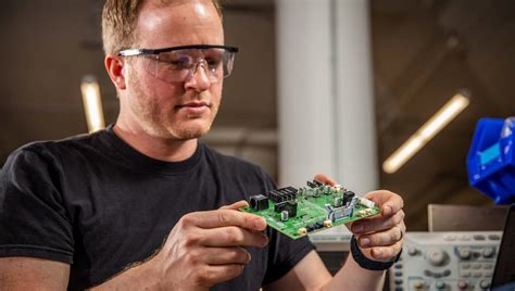
24-Hour Prototyping for Complex PCB Designs
When working with intricate PCB layouts requiring high-density interconnects or specialized materials, time-sensitive prototyping often becomes a critical bottleneck. Leading PCB manufacturing companies now address this challenge by offering round-the-clock production cycles that compress traditional 2–3 week lead times into a single day. This acceleration is achieved through automated design validation systems that cross-reference your schematics against PCB manufacturing cost drivers like layer counts, via types, and material grades in real time.
You’ll find these services particularly valuable when iterating advanced designs with 16+ layers or embedded components. Advanced PCB manufacturing platforms employ machine learning algorithms to predict fabrication challenges before submitting files, reducing revision loops by up to 70%. For prototypes involving RF shielding or impedance-controlled traces, instant DFM (Design for Manufacturability) feedback ensures your technical specifications align with the PCB manufacturing business’s capabilities from the first iteration.
The process integrates seamlessly with your existing workflow:
- Upload design files with automated impedance calculations
- Receive material compatibility alerts within 15 minutes
- Confirm prototype parameters through interactive 3D board visualization
- Lock in pricing with guaranteed no-change clauses
This operational model proves especially effective for medical IoT or aerospace prototypes where thermal management and signal integrity can’t be compromised. By eliminating traditional back-and-forth communication cycles, you maintain control over both timelines and budgets—critical when dealing with advanced substrates like Rogers 4350B or polyimide flex circuits.
For teams managing concurrent projects, the 24-hour window allows parallel testing of multiple design variants. This approach reduces opportunity costs associated with delayed product validations, particularly when coordinating with global component suppliers. Modern PCB manufacturing cost structures further support this agility, offering tiered pricing that scales with your prototyping frequency rather than forcing bulk commitments.
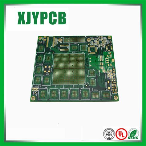
Bulk PCB Production for 10,000 Pad Projects
When scaling up to PCB manufacturing for projects requiring 10,000+ pads, efficiency and precision become non-negotiable. Leading PCB manufacturing companies leverage advanced automated workflows to handle high-density designs without compromising turnaround times. By integrating design-for-manufacturability (DFM) checks early in the process, these systems flag potential issues like trace spacing violations or thermal imbalances—critical for avoiding costly rework in bulk orders.
"For large-scale projects, partnering with a PCB manufacturing business that offers tiered pricing models can significantly reduce PCB manufacturing cost per unit. Always request a detailed breakdown of material, labor, and tooling fees to optimize your budget."
Modern online platforms simplify volume production by providing instant quotes based on real-time component availability and layer counts. For example, specifying a 12-layer board with HDI (high-density interconnect) technology might increase initial costs but ensures reliability for complex applications like industrial automation or medical devices. Pro tip: Use parametric search filters to compare lead times and pricing across different PCB manufacturing service tiers—this helps balance speed and affordability.
Supply chain transparency is another key advantage. Reputable providers share live updates on material sourcing, fabrication milestones, and assembly progress, letting you adjust timelines if delays arise. This is particularly valuable when managing just-in-time inventory strategies or coordinating with third-party logistics partners.
Finally, consider sustainability. Many PCB manufacturing companies now offer eco-friendly options, such as lead-free finishes or recyclable substrates, which align with corporate ESG goals while maintaining performance standards. By aligning your bulk production needs with a provider’s technical capabilities and ethical practices, you ensure scalability without sacrificing quality.
Streamlined PCB Design Process for Faster Results
Modern PCB manufacturing workflows demand precision and speed, which begins with an optimized design phase. By leveraging cloud-based collaboration tools, you can iterate designs in real time with engineers and PCB manufacturing companies, eliminating redundant feedback loops. Advanced design rule checks (DRCs) automatically flag issues like trace spacing violations or impedance mismatches, reducing post-design revisions by up to 70%. Component libraries pre-validated by manufacturers ensure your schematic aligns with available parts, preventing delays caused by obsolete or out-of-stock items.
Integrated platforms sync your design files directly with PCB manufacturing cost estimators, allowing you to adjust layer counts or materials for budget optimization. For instance, switching from FR-4 to high-frequency substrates mid-design triggers instant recalculations, empowering data-driven decisions. This integration is particularly critical for complex projects, where even minor layout changes can impact fabrication timelines by days.
When preparing for bulk runs, automated panelization tools maximize board yield per panel—a key factor in scaling PCB manufacturing business operations. Features like tear-off tabs and mouse bite placements are generated algorithmically, ensuring compatibility with assembly machinery. Real-time DFM (design for manufacturability) analysis further bridges the gap between prototyping and mass production, flagging issues like insufficient solder mask clearance before files reach the factory.
By unifying design and fabrication workflows, you bypass manual file conversions and miscommunication risks. This end-to-end visibility lets you prioritize speed-to-market without compromising on quality—whether you’re producing 10 prototypes or 10,000 high-density boards.
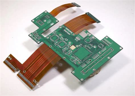
Integrated PCB Manufacturing & Assembly Services
When scaling your electronics project, PCB manufacturing and assembly often present logistical hurdles. Modern integrated service providers eliminate these challenges by combining design, fabrication, and component assembly into a single workflow. This approach ensures seamless coordination between your design files and the physical board, reducing errors and accelerating timelines.
Leading PCB manufacturing companies now offer real-time tracking for every stage—from material procurement to final testing. You can monitor production milestones, adjust component choices based on availability, and validate PCB manufacturing cost estimates before committing to bulk orders. For projects requiring precision, automated optical inspection (AOI) and X-ray verification ensure even densely packed boards with 10,000+ pads meet industry standards.
The synergy between PCB manufacturing business operations and assembly services also simplifies sourcing. Instead of managing multiple vendors, integrated platforms provide access to certified components, minimizing supply chain delays. For example, if your design requires specialized ICs or connectors, in-house inventory networks cross-reference global databases to secure parts at competitive rates.
Cost efficiency extends beyond materials. By merging fabrication and assembly, you avoid markup fees from third-party partners. Advanced platforms even optimize panel layouts to reduce waste during PCB manufacturing, lowering per-unit expenses for large batches. For startups or enterprises, this scalability ensures prototypes and mass production align with budget constraints without compromising quality.
Ultimately, choosing a provider that unites design support, PCB manufacturing, and assembly under one digital roof streamlines complexity. You gain visibility into every variable—from lead times to compliance certifications—while focusing on innovation rather than logistics.
Expert PCB Design Support for Large-Scale Projects
Navigating PCB manufacturing for high-density, large-scale projects demands precision and specialized expertise. When your design involves 10,000+ pads or multilayer architectures, even minor oversights in trace routing or component placement can escalate PCB manufacturing costs and delay timelines. This is where partnering with seasoned PCB manufacturing companies becomes critical. Their engineering teams analyze your schematics through design for manufacturing (DFM) lenses, identifying potential bottlenecks like impedance mismatches or thermal hotspots before prototyping begins.
For complex layouts, these experts often recommend optimizing panelization strategies to reduce material waste—a key factor in controlling PCB manufacturing business expenses. Advanced tools like automated design rule checks (DRC) ensure compliance with fabrication tolerances, while signal integrity simulations validate performance under real-world conditions. You’ll also gain access to component substitution guidance, which helps mitigate supply chain risks without compromising functionality.
Large-scale production runs require seamless coordination between design and manufacturing workflows. Leading providers integrate real-time collaboration platforms where you can review design iterations, adjust stack-ups, or approve material substitutions alongside their engineers. This proactive approach minimizes rework cycles and ensures your high-pad-count designs transition smoothly from prototype validation to full-scale PCB manufacturing. By aligning design choices with production capabilities early, you avoid costly mid-process revisions—keeping projects on schedule and within budget.
For mission-critical applications, some PCB manufacturing companies offer dedicated account managers who oversee every technical detail, from thermal management solutions to impedance-controlled routing. This level of support is particularly valuable when scaling prototypes into bulk orders, as it ensures consistency across thousands of boards while maintaining stringent quality benchmarks. With expert guidance, you’re not just outsourcing fabrication—you’re leveraging decades of collective experience to refine designs for manufacturability, reliability, and cost-efficiency.
Online PCB Design Tools with Instant Quoting
Modern platforms now integrate PCB manufacturing workflows directly into design interfaces, allowing you to generate real-time quotes while drafting layouts. These tools automatically cross-reference component availability from partnered PCB manufacturing companies, eliminating guesswork about part shortages or lead times. As you route traces or place vias, built-in calculators update PCB manufacturing cost estimates based on material choices, layer counts, and finish options—giving you immediate visibility into budget impacts.
Advanced features like automated design rule checks (DRC) prevent costly revisions by flagging spacing errors or impedance mismatches before submission. For complex designs, some platforms offer collaboration portals where your team and the PCB manufacturing business engineers can annotate files, ensuring alignment on tolerances or stack-up requirements. This seamless handoff reduces back-and-forth emails and accelerates approval cycles by 40–60% compared to traditional methods.
The best systems also provide supply chain dashboards that track component pricing trends, helping you decide whether to substitute parts or lock in bulk pricing. When prototyping, instant quoting tools automatically prioritize faster turnaround options, while high-volume orders for 10,000+ pad projects trigger volume discounts from partnered manufacturers. By centralizing design and PCB manufacturing logistics, these platforms turn weeks of coordination into a single, streamlined workflow—letting you focus on innovation rather than administrative tasks.
Conclusion
By integrating PCB manufacturing into a unified digital platform, you eliminate the friction traditionally associated with bringing complex designs to life. Modern PCB manufacturing companies leverage cloud-based tools to provide real-time visibility into PCB manufacturing cost, allowing you to optimize budgets while scaling from prototypes to high-volume orders. For projects requiring up to 10,000+ pads, this streamlined approach ensures consistent quality across bulk production runs without compromising speed—a critical advantage in fast-paced industries.
The synergy between design and PCB manufacturing business operations is further enhanced by intelligent component selection systems, which automatically flag supply chain risks and suggest alternatives. Cost predictability becomes achievable when quoting engines analyze material availability, layer counts, and lead times in seconds. Whether you’re iterating a prototype in 24 hours or coordinating global manufacturing workflows, these platforms centralize communication, reducing errors and accelerating time-to-market.
Ultimately, the shift toward end-to-end online solutions redefines how engineers and businesses approach PCB manufacturing. By combining expert design validation with agile production capabilities, you gain the flexibility to tackle both niche projects and large-scale deployments—all while maintaining control over timelines, specifications, and budgets.
FAQs
How do PCB manufacturing costs vary between prototype and bulk orders?
Typical pricing models charge a premium for low-volume prototypes due to setup fees, but PCB manufacturing companies often reduce per-unit costs by 30–60% for bulk orders exceeding 1,000 units. Factors like material choice, layer count, and surface finish also impact final pricing.
What should you look for in PCB manufacturing companies for large-scale projects?
Prioritize vendors with proven expertise in handling high-density interconnect (HDI) designs and 10,000+ pad layouts. Certifications like ISO 9001 and IPC-A-610 Class 3 ensure adherence to industrial standards, while real-time production tracking minimizes delays.
Can PCB manufacturing business services integrate with custom design tools?
Most providers offer API-based integrations, allowing seamless data transfer between your design software and their PCB manufacturing systems. This eliminates manual file uploads and ensures instant quoting accuracy for complex designs.
How do you balance PCB manufacturing cost with quality for budget-sensitive projects?
Opt for standardized materials like FR-4 substrates and avoid exotic finishes unless necessary. Many companies provide design-for-manufacturing (DFM) checks to identify cost-saving adjustments without compromising functionality.
What turnaround times can you expect from PCB manufacturing companies for urgent orders?
Leading suppliers offer 24-hour prototyping for designs up to 8 layers, while bulk orders typically ship within 5–7 business days. Expedited services may incur a 15–25% surcharge but ensure faster delivery for time-critical projects.
Ready to Optimize Your PCB Manufacturing Workflow?
Streamline your next project with end-to-end solutions—click here to explore tailored services.