Optimizing Assembly Circuit Reliability Through Advanced Design Principles

Key Takeaways
Effective PCB assembly and PCBA reliability hinge on three core pillars: thermal management, material precision, and error-proofing methodologies. Optimizing thermal stability during PCB assembly prevents component degradation, particularly in high-power applications, by balancing heat dissipation with controlled operating temperatures. Selecting high-grade substrates and low-thermal-expansion alloys ensures structural integrity across temperature cycles, a critical factor in PCBA longevity.
Equally critical are error-proofing techniques, such as automated optical inspection (AOI) and design-for-manufacturability (DFM) checks, which minimize defects in PCB assembly workflows. These strategies align with failure mode analysis to preemptively address risks like solder joint fractures or signal interference. For mission-critical systems—from aerospace to medical devices—integrating these principles into PCBA design elevates operational resilience, reducing downtime and lifecycle costs. By harmonizing advanced thermal solutions, precision materials, and robust validation protocols, engineers systematically mitigate failure risks while enhancing the durability and performance of modern electronic assemblies.
Thermal Management in Circuit Assembly
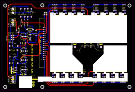
Effective thermal management in PCB assembly ensures long-term reliability by addressing heat generation and dissipation challenges inherent in modern electronics. High-power components, such as processors or voltage regulators, generate significant heat during operation, which, if unmanaged, accelerates material degradation and increases failure risks. To mitigate this, designers employ thermal vias and copper pours to enhance heat transfer away from critical areas in PCBA layouts. Additionally, selecting substrates with high thermal conductivity, like metal-core or ceramic-filled laminates, improves heat distribution while maintaining structural integrity.
Advanced thermal simulation tools enable precise modeling of heat flow patterns, allowing engineers to optimize component placement and airflow pathways before prototyping. For instance, integrating heat sinks or thermally conductive adhesives in PCB assembly can reduce junction temperatures by up to 30%, directly extending component lifespan. Transitioning to the next design phase, these thermal strategies align with error-proofing techniques by preemptively identifying hotspots that could lead to solder joint fatigue or delamination. By balancing thermal efficiency with mechanical constraints, PCBA designs achieve thermal stability without compromising performance in demanding environments.
Precision Materials for Reliable Circuits
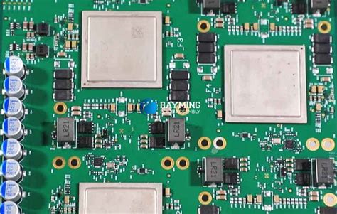
The foundation of durable PCB assembly lies in the strategic selection of materials that balance electrical performance, thermal resilience, and mechanical stability. In PCBA (Printed Circuit Board Assembly), substrates like high-Tg FR-4 or polyimide-based laminates are prioritized for their ability to withstand elevated temperatures while maintaining structural integrity. Conductive materials, such as oxygen-free copper traces or silver-loaded epoxy adhesives, ensure minimal signal loss and robust connectivity, even under cyclic stress.
| Material Type | Key Properties | Application Example |
|---|---|---|
| High-Tg FR-4 | Thermal stability (>170°C), low moisture absorption | Multilayer boards for industrial controls |
| Ceramic-filled PTFE | Ultra-low dielectric loss, high-frequency stability | RF/microwave circuits in telecommunications |
| Lead-free solder alloys | RoHS compliance, reduced thermal fatigue | Consumer electronics PCBA |
Advanced coatings, including parylene conformal films or silicone-based encapsulants, further shield circuits from environmental hazards like humidity and chemical exposure. For mission-critical systems, material choices are validated through accelerated life testing to simulate decades of operational stress within weeks. By aligning PCB assembly workflows with precision material science, engineers systematically reduce latent defects and extend the functional lifespan of electronic systems.
Error-Proofing Techniques in Circuit Design
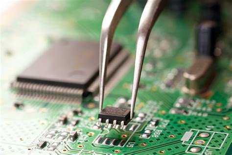
Implementing robust error-proofing techniques is essential for minimizing defects in PCB assembly processes. Modern design-for-manufacturability (DFM) principles prioritize layout optimizations that reduce human error risks, such as asymmetrical component footprints or polarized connector markings. Automated optical inspection (AOI) systems, integrated into PCBA production lines, scan boards at micron-level precision to detect soldering anomalies or misplaced components before final testing.
Tip: Incorporate redundant alignment markers and standardized silkscreen labels during the design phase to streamline assembly workflows and reduce rework rates.
Advanced software tools now simulate thermal and mechanical stresses across PCB assembly layers, flagging potential failure points like trace fractures or via misalignments. For mission-critical applications, fault-tree analysis (FTA) models preemptively identify single-point failures, guiding designers to implement parallel circuits or error-correcting code (ECC) memory architectures. Cross-functional collaboration between design and manufacturing teams ensures PCBA layouts align with production capabilities, balancing complexity with reliability.
By embedding error-proofing protocols early in the design cycle, engineers achieve higher first-pass yield rates while maintaining compliance with industry standards such as IPC-A-610. This proactive approach not only reduces costly post-production corrections but also strengthens long-term performance in demanding operational environments.
Circuit Reliability for Critical Applications
In industries where system failures carry catastrophic consequences—such as aerospace, medical devices, or industrial automation—ensuring circuit reliability demands meticulous adherence to advanced design protocols. PCB assembly processes (PCBA) must prioritize environmental resilience and signal integrity, particularly when circuits operate under extreme temperatures, vibrations, or electromagnetic interference. For instance, mission-critical applications often require multi-layered redundancy in PCBA layouts, coupled with rigorous testing for thermal cycling and mechanical stress endurance.
A key strategy involves integrating failure mode analysis during the PCB assembly phase to preemptively identify weak points, such as solder joint fatigue or trace delamination. Materials selection also plays a pivotal role; high-grade substrates with low thermal expansion coefficients and conductive adhesives rated for harsh environments significantly enhance longevity. Furthermore, error-proofing techniques like automated optical inspection (AOI) ensure microscopic defects are detected before deployment.
Transitioning seamlessly from design to execution, engineers must align PCBA workflows with industry-specific standards (e.g., IPC-A-610 for aerospace), ensuring compliance without compromising operational efficiency. By embedding reliability-centric practices at every stage—from schematic design to final assembly circuit validation—manufacturers can mitigate risks while maintaining the precision required for life-critical systems.
Advanced Design Principles for Circuits
Implementing advanced design principles in PCB assembly requires a holistic approach that balances electrical performance, mechanical durability, and environmental resilience. At the core of these principles lies signal integrity optimization, which ensures minimal interference in high-frequency applications through controlled impedance routing and proper grounding strategies. For PCBA reliability, material selection extends beyond basic conductivity—engineers prioritize high-Tg substrates and low-loss dielectrics to withstand thermal cycling and humidity fluctuations.
Thermal management is further refined using embedded heat sinks and thermal vias, which dissipate heat efficiently without compromising circuit density. Advanced design for manufacturability (DFM) guidelines also play a pivotal role, aligning component placement with automated assembly processes to reduce solder joint defects. Additionally, failure mode and effects analysis (FMEA) is integrated early in the design phase to preemptively address potential weak points, such as voltage spikes or mechanical stress concentrations.
Transitioning to error-proofing, polarization markers and asymmetric component footprints prevent misalignment during PCB assembly, while redundant power pathways enhance fault tolerance in mission-critical PCBA systems. These strategies not only align with industry standards like IPC-6012 but also ensure scalability for evolving technological demands. By harmonizing these methodologies, designers create circuits that excel in both immediate functionality and long-term operational stability.
Mitigating Circuit Failure Risks Strategically
Strategic mitigation of circuit failure begins with a holistic approach to PCB assembly design, integrating proactive risk assessment with robust engineering practices. A critical focus lies in addressing thermal stressors, which account for over 40% of PCBA failures in high-performance systems. By embedding predictive thermal modeling during layout planning, engineers can preemptively identify hotspots and adjust trace widths or copper weights to enhance heat dissipation. Concurrently, selecting low-thermal-expansion substrates minimizes mechanical strain caused by temperature fluctuations, a common failure mode in mission-critical applications like aerospace or medical devices.
Error-proofing extends beyond component placement accuracy. Implementing automated optical inspection (AOI) systems at multiple PCB assembly stages ensures microscopic defects—such as solder bridging or tombstoning—are detected before final integration. For PCBA destined for harsh environments, conformal coating techniques combined with accelerated life testing validate resilience against moisture, vibration, and chemical exposure. Additionally, adopting failure mode and effects analysis (FMEA) frameworks enables systematic prioritization of risks, aligning design choices with application-specific reliability thresholds.
Crucially, collaboration between material scientists and electrical engineers ensures synergistic optimization of conductive inks, dielectric layers, and interconnect geometries. This multidisciplinary strategy not only reduces latent defects but also elevates mean time between failures (MTBF) by up to 30%, as evidenced by recent industry case studies.
Optimizing Assembly for Circuit Longevity
Achieving long-term reliability in PCB assembly requires meticulous attention to manufacturing processes and material interactions. Central to this effort is the integration of precision soldering techniques that minimize thermal stress on components during PCBA workflows. By employing automated optical inspection (AOI) systems and controlled reflow profiles, manufacturers can ensure consistent solder joint integrity—a critical factor in preventing micro-cracks and intermittent failures.
Material compatibility plays an equally critical role. Selecting low-voiding underfill materials and high-Tg substrates enhances resistance to thermal cycling, particularly in applications exposed to extreme temperatures. Advanced PCB assembly lines now leverage predictive modeling to simulate stress distribution across multilayer boards, enabling preemptive adjustments to component placement and trace routing.
Error-proofing extends beyond design validation. Implementing failsafe protocols in PCBA workflows—such as polarity verification and moisture-sensitive component handling—reduces latent defects that might compromise longevity. Furthermore, pairing these measures with rigorous environmental testing (e.g., HALT/HASS) ensures circuits withstand operational stressors without degradation.
By harmonizing precision manufacturing with proactive failure analysis, engineers systematically extend the service life of electronic systems while maintaining alignment with industry reliability benchmarks.
Thermal Stability in Circuit Assembly
Ensuring thermal stability in PCB assembly begins with understanding how temperature fluctuations impact material behavior and electrical performance. Modern high-power-density designs in PCBA demand precise thermal management strategies, as even a 10°C temperature rise can accelerate component aging by 50% in mission-critical systems. Engineers employ finite element analysis to simulate heat distribution patterns, identifying hotspots where thermal interface materials or copper-thickness adjustments are needed.
A key innovation involves using thermally conductive substrates with low coefficients of thermal expansion (CTE), which maintain dimensional stability across operating temperatures ranging from -40°C to 125°C. For example, polyimide-based laminates in PCB assembly reduce warping risks by 30% compared to standard FR-4 materials, particularly in multilayer configurations. Additionally, active cooling solutions such as embedded heat pipes or microchannel arrays are increasingly integrated into PCBA layouts for applications like automotive power electronics.
Transitioning to manufacturing, reflow profiling ensures solder joints withstand thermal cycling stresses. By optimizing peak temperatures and ramp rates during soldering, manufacturers achieve void rates below 5% in BGA connections, significantly improving long-term reliability. This focus on thermal resilience directly supports the subsequent discussion on material selection, creating a cohesive framework for mitigating failure risks across the product lifecycle.
Conclusion
The pursuit of PCB assembly reliability hinges on integrating advanced design principles that address both technical and operational challenges. By prioritizing thermal stability through optimized heat dissipation strategies—such as copper balancing and strategic component placement—engineers can mitigate thermal stress in PCBA systems. Equally critical is the selection of precision materials, including high-grade substrates and solder alloys, which ensure durability under fluctuating environmental conditions. Error-proofing techniques, such as automated optical inspection (AOI) and redundant circuit pathways, further reduce failure risks by identifying defects early in the assembly circuit process.
For mission-critical applications, these principles coalesce to extend operational lifespans while maintaining performance consistency. The interplay between thermal management, material science, and design foresight underscores the importance of a holistic approach in PCB assembly workflows. As industries demand higher reliability from PCBA systems, adopting these methodologies not only safeguards against premature failures but also aligns with evolving standards for electronics resilience. Ultimately, the integration of these strategies ensures that assembly circuits meet the rigorous demands of modern technology, from aerospace to medical devices, where precision and longevity are non-negotiable.
FAQs
How does thermal management impact PCB assembly reliability?
Effective thermal management in PCBA ensures components operate within safe temperature ranges, preventing overheating-induced failures. Techniques like thermal vias, heatsinks, and optimized trace layouts are critical for maintaining long-term stability in high-power applications.
What materials enhance precision in circuit assembly?
Selecting low-thermal-coefficient substrates and high-conductivity solders minimizes expansion mismatches and resistive losses. Materials like FR-4 with ceramic fillers or polyimide-based laminates are preferred for PCB assembly in harsh environments.
Can error-proofing techniques reduce manufacturing defects?
Yes, automated optical inspection (AOI) and design-for-manufacturability (DFM) checks identify layout flaws early. Implementing foolproof connector orientations and standardized footprints in PCBA designs significantly lowers assembly errors.
Why is reliability critical for mission-critical systems?
Failures in aerospace, medical, or industrial PCB assemblies can lead to catastrophic outcomes. Redundant circuits, rigorous testing protocols, and environmentally resistant coatings ensure compliance with stringent industry standards.
How do advanced design principles improve circuit longevity?
Simulation-driven approaches, such as finite element analysis (FEA) and stress testing, predict failure modes. Pairing these with robust component placement and derating strategies extends the operational lifespan of PCBA systems.
Ready to Optimize Your PCB Assembly Process?
For tailored solutions in high-reliability PCB assembly, please click here to explore advanced design services and technical support.