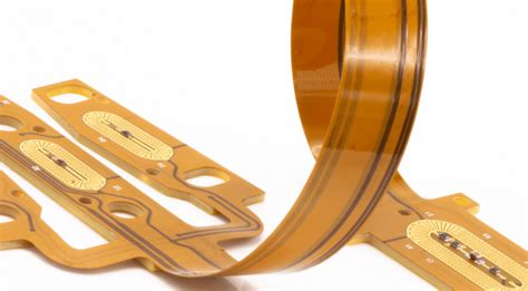
Optimizing Assy PCB Assembly for High-Density Electronic Systems

Key Takeaways
Effective optimization of PCB assembly processes for high-density electronic systems requires addressing multiple interdependent factors. Proper thermal management strategies—such as incorporating thermal vias or heat sinks—are critical to prevent overheating in compact PCBA designs. Equally vital is optimizing component placement to minimize signal path lengths and reduce electromagnetic interference, directly enhancing signal integrity.
When selecting materials for PCB assembly, advanced substrates with high glass transition temperatures (Tg) and low dielectric loss improve performance in demanding environments. Below is a comparison of conventional versus advanced materials:
| Property | Conventional FR-4 | Advanced Polyimide |
|---|---|---|
| Thermal Conductivity | 0.3 W/mK | 0.5 W/mK |
| Dielectric Constant | 4.5 | 3.2 |
| Max Operating Temp | 130°C | 260°C |
To ensure reliability, manufacturers must prioritize automated optical inspection (AOI) and X-ray testing during PCBA production. Additionally, adhering to design-for-manufacturability (DFM) principles reduces risks of soldering defects or misalignments in high-density layouts. By balancing material innovation, precision assembly, and rigorous testing, engineers can achieve optimal performance in complex PCB assembly projects.

Thermal Management in High-Density Assy PCBs
Effective thermal management is critical in PCB assembly for high-density electronic systems, where compact layouts and increased power demands amplify heat generation. Without proper dissipation, excessive temperatures can degrade component performance, reduce lifespan, or cause catastrophic failures. Key strategies include optimizing thermal vias—plated holes that transfer heat to inner or backside copper layers—and selecting materials with high thermal conductivity, such as metal-core substrates or advanced ceramics.
Tip: Integrate thermal simulations early in the PCBA design phase to identify hotspots and validate heat-spreading solutions like embedded heat sinks or liquid cooling channels.
Component placement also plays a pivotal role. High-power devices should be positioned away from thermally sensitive parts, and thermal relief pads can mitigate soldering defects while maintaining heat flow. Additionally, using thermally conductive adhesives or epoxy underfills enhances heat transfer from chips to the board. For multilayer designs, balancing the coefficient of thermal expansion (CTE) across materials prevents mechanical stress during temperature cycling.
Advanced PCB assembly techniques, such as staggered via patterns and copper pours, further improve thermal performance without compromising signal integrity. By combining material science, layout optimization, and predictive modeling, engineers can ensure reliable operation even in the most demanding high-density environments.

Optimizing Component Placement for Signal Integrity
Effective PCB assembly for high-density systems requires meticulous attention to component placement to mitigate signal degradation and electromagnetic interference (EMI). In PCBA designs, high-speed digital components and sensitive analog circuits must be strategically positioned to minimize trace lengths and avoid parallel routing of critical signals. For instance, placing clock generators away from data lines reduces crosstalk, while grouping power regulation modules near their load sources minimizes voltage drops.
A key strategy involves partitioning the board into functional zones—separating noisy digital sections from analog or RF areas—using ground planes as shielding barriers. This approach not only enhances signal integrity but also simplifies thermal management by clustering heat-generating components in designated regions. Additionally, adhering to design-for-manufacturability (DFM) principles ensures that densely packed components remain accessible for automated assembly and inspection.
Transitioning between layout phases, engineers should leverage PCBA simulation tools to model signal propagation delays and impedance mismatches. Iterative adjustments, such as optimizing via placement and reducing stub lengths, further refine performance. By balancing spatial constraints with electrical requirements, designers can achieve robust PCB assembly outcomes that meet the demands of modern high-density electronics.
Ensuring Reliability in Assy PCB Assembly Processes
Achieving consistent reliability in PCB assembly for high-density systems demands rigorous attention to process controls and material compatibility. Thermal cycling, vibration resistance, and moisture exposure are critical stressors that can compromise PCBA longevity, particularly in compact designs. To mitigate these risks, manufacturers prioritize automated optical inspection (AOI) and X-ray testing to detect soldering defects, such as voids or misaligned components, which are common failure points in densely packed layouts.
Material selection plays a pivotal role, with high-temperature laminates and low-voiding solder pastes enhancing thermal stability and electrical connectivity. Additionally, conformal coatings are applied to shield sensitive components from environmental contaminants, ensuring PCB assembly integrity under harsh operating conditions. Process optimization, including precise reflow profiles and controlled atmosphere soldering, minimizes thermal stress during PCBA fabrication.
Collaboration between design and manufacturing teams is essential to align component placement with assembly feasibility, reducing mechanical strain on interconnects. By integrating these practices, engineers can systematically address reliability challenges while maintaining alignment with broader goals of signal integrity and thermal management in high-density electronics.

Advanced Materials for High-Performance Assy PCBs
The selection of advanced materials plays a pivotal role in enhancing the performance and reliability of PCB assembly (PCBA) in high-density electronic systems. Modern high-Tg (glass transition temperature) laminates, such as polyimide or ceramic-filled substrates, are increasingly adopted to withstand elevated operating temperatures while maintaining structural stability. These materials reduce thermal stress during reflow soldering, a critical consideration for PCBA in compact designs. For applications demanding high-frequency operation, low-loss dielectrics like Rogers or PTFE-based substrates minimize signal attenuation, directly addressing signal integrity challenges outlined earlier.
To optimize thermal management, thermally conductive prepregs or metal-core substrates are integrated into PCB assembly layers, enabling efficient heat dissipation without compromising board thickness. Additionally, halogen-free laminates are gaining traction due to their environmental compliance and improved flame retardancy, aligning with industry sustainability trends. For high-reliability applications, advanced underfill materials and conductive adhesives enhance mechanical stability in PCBA, particularly for fine-pitch components.
These material innovations not only support miniaturization but also ensure compatibility with automated PCB assembly processes, bridging the gap between performance demands and manufacturability. By leveraging these advancements, engineers can mitigate risks associated with thermal cycling and mechanical fatigue, ultimately extending the operational lifespan of high-density electronic systems.

Signal Integrity Challenges in Compact PCB Designs
Maintaining signal integrity in compact PCB assembly designs requires addressing multiple interrelated factors. As component density increases in modern high-performance electronics, issues like crosstalk, electromagnetic interference (EMI), and impedance mismatches become critical. Tightly packed traces and reduced spacing between layers in PCBA layouts amplify capacitive coupling, leading to unintended signal distortion. To mitigate these effects, engineers must prioritize controlled impedance routing and strategic use of ground planes to isolate high-speed signals.
Advanced simulation tools play a pivotal role in predicting signal behavior during the PCB assembly phase, enabling preemptive adjustments to trace geometries and via placements. For instance, minimizing stubs in high-frequency paths and adopting differential pair routing can reduce reflections and noise. Additionally, material selection—such as low-loss laminates with stable dielectric constants—directly impacts signal attenuation, especially in millimeter-wave applications.
Thermal management also intersects with signal integrity, as temperature fluctuations in densely populated PCBA designs can alter material properties and impedance characteristics. Integrating thermal vias near heat-generating components helps stabilize performance while maintaining signal paths. Finally, rigorous testing protocols, including time-domain reflectometry (TDR) and eye diagram analysis, validate design choices and ensure compliance with signal integrity benchmarks in compact layouts.
Best Practices for High-Density Assy PCB Layouts
Effective PCB assembly for high-density systems demands meticulous attention to layout design. A well-structured PCBA begins with optimizing component placement to minimize signal path lengths and reduce electromagnetic interference (EMI). Prioritize high-speed signal paths by routing them first, ensuring they follow direct, uninterrupted trajectories. Use microvia technology to accommodate fine-pitch components, which is critical for maintaining signal integrity in compact designs.
Thermal management must be integrated into the layout phase. Distribute heat-generating components evenly and incorporate thermal relief pads to prevent solder joint stress during reflow. Pairing this with copper pours or embedded heat sinks enhances heat dissipation, aligning with broader strategies for thermal management in high-density systems.
Layer stack-up planning is equally vital. Opt for symmetrical layer configurations to avoid warping and ensure consistent impedance control. For mixed-signal designs, isolate analog and digital grounds using split planes or moats, reducing noise coupling. Finally, leverage automated design rule checks (DRCs) to validate clearances, trace widths, and via placements, ensuring compliance with high-density PCB assembly standards. By balancing these practices, designers can achieve reliable, high-performance layouts that meet the demands of modern electronics.
Maximizing Performance Through Assy PCB Optimization
Achieving peak performance in PCB assembly for high-density systems demands a holistic approach that integrates electrical, thermal, and mechanical considerations. At the core of PCBA optimization lies the strategic balancing of component density with signal integrity requirements. Designers must prioritize controlled impedance routing for high-speed traces while minimizing crosstalk through careful spacing and shielding. Simultaneously, optimizing thermal management—such as integrating thermal vias or selecting substrates with superior heat dissipation—ensures stable operation under demanding conditions.
A critical step involves leveraging advanced simulation tools to model signal integrity and power distribution networks before finalizing layouts. This preemptive analysis helps identify bottlenecks like voltage drops or electromagnetic interference (EMI), enabling iterative refinements. For PCB assembly processes, adopting laser-drilled microvias and sequential lamination techniques supports finer pitch components, essential for compact designs. Additionally, material selection plays a pivotal role; high-Tg laminates and low-loss dielectrics enhance reliability in thermally stressful environments.
Transitioning from design to production, rigorous testing protocols—such as automated optical inspection (AOI) and in-circuit testing (ICT)—validate PCBA quality. By aligning design choices with manufacturing capabilities, engineers can mitigate risks like solder joint fatigue or delamination. This synergy between innovation and precision ensures that optimized Assy PCB solutions meet the exacting demands of modern high-density electronics.
Addressing Heat Dissipation in Assy PCB Assemblies
Effective thermal management is critical in PCB assembly for high-density electronic systems, where increased component density amplifies heat generation. Thermal stress remains a leading cause of failure in PCBA, making proactive heat dissipation strategies essential. Designers often integrate thermal vias and copper pours to distribute heat evenly, while advanced substrates like metal-core or ceramic-based laminates enhance thermal conductivity.
Component placement plays a dual role here: positioning high-power devices near board edges or heatsinks improves airflow, whereas isolating heat-sensitive components minimizes performance degradation. For compact layouts, simulation tools such as computational fluid dynamics (CFD) help model heat flow patterns, enabling precise optimization of PCB assembly geometries.
Additionally, selecting low-thermal-resistance materials for solder masks and adhesives ensures efficient heat transfer between layers. In PCBA processes, techniques like selective soldering reduce thermal exposure to adjacent components, preserving integrity. Finally, post-assembly validation through infrared thermography identifies hotspots, allowing iterative refinements to balance thermal performance with signal integrity in space-constrained designs.
Conclusion
In the pursuit of high-performance PCB assembly for high-density electronic systems, balancing thermal, electrical, and mechanical demands remains paramount. Optimizing PCBA processes requires meticulous attention to signal integrity, thermal management, and component placement—each playing a critical role in ensuring long-term reliability. Advanced materials, such as high-Tg substrates and low-loss dielectrics, further enhance performance in compact designs, while robust assembly protocols mitigate risks like solder joint fatigue or thermal stress.
For engineers, adopting a holistic approach—from layout simulation to post-assembly testing—ensures that high-density designs meet stringent operational standards. Partnering with experienced providers, such as RPC Electronics, can streamline the integration of cutting-edge techniques into PCB assembly workflows. Ultimately, the convergence of precision engineering and innovative material science will continue to drive advancements in PCBA, enabling next-generation electronics to thrive in increasingly demanding environments.
FAQs
What thermal management techniques are critical for high-density PCB assembly?
Effective thermal management in PCBA relies on thermal vias, copper pours, and advanced heatsink materials. Implementing impedance-controlled routing and selecting low-CTE substrates further mitigate heat accumulation in compact layouts.
How does component placement affect signal integrity in PCB assembly?
Strategic placement minimizes crosstalk and electromagnetic interference (EMI). Grouping high-speed components near voltage regulators and maintaining proper trace spacing are essential for preserving signal quality in high-density PCBA.
What material choices enhance reliability in high-performance PCBA?
High-Tg laminates, polyimide substrates, and halogen-free prepregs improve thermal stability and mechanical durability. These materials reduce delamination risks and support finer pitch components in dense PCB assemblies.
Why is impedance matching vital for compact PCB designs?
Mismatched impedance causes signal reflections and data errors, particularly in high-speed circuits. Using controlled-depth microvias and optimized dielectric stackups ensures consistent impedance across miniaturized PCBA layouts.
How do reflow soldering profiles impact assembly reliability?
Precise temperature gradients prevent tombstoning and solder voids. For mixed-technology PCBA, dual-stage reflow processes accommodate both SMDs and through-hole components while reducing thermal stress.
Explore Advanced Solutions for Your PCB Assembly Needs
For tailored strategies in optimizing high-density PCBA, please click here to consult our engineering team and access cutting-edge design resources.

