Optimizing Circuit Performance with Embedded PCB Integration
Key Takeaways
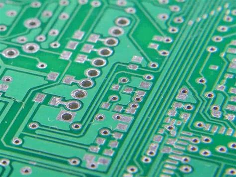
When working with PCB manufacturing companies, you’ll find that embedded PCB manufacturing prioritizes three-dimensional integration to minimize parasitic effects—a common challenge in traditional designs. By embedding active and passive components directly into the substrate, PCB manufacturing costs can be optimized through reduced material waste and simplified assembly workflows. This approach not only enhances thermal dissipation but also allows for tighter component spacing, improving signal integrity in high-frequency applications.
For businesses evaluating PCB manufacturing business models, embedded designs offer scalability. Advanced processes like laser-drilled microvias and sequential lamination enable precise 3D stacking, which lowers electromagnetic interference (EMI) risks. Additionally, thermal vias and conductive adhesives address heat buildup, ensuring reliability in dense layouts.
While upfront investments in PCB manufacturing for embedded systems may seem higher, long-term savings emerge from fewer interconnects and improved yield rates. To stay competitive, prioritize partners adept in 3D substrate integration, as their expertise directly impacts performance optimization and cost efficiency. Understanding these principles helps you navigate the shift from conventional boards to next-generation embedded solutions.
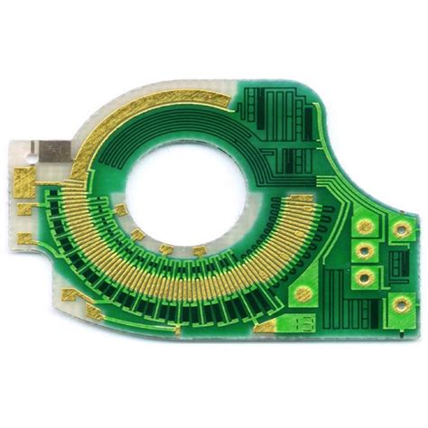
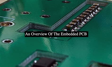
Embedded PCB Manufacturing for Enhanced Circuit Efficiency
When designing high-performance electronics, PCB manufacturing techniques play a critical role in balancing efficiency and functionality. By embedding components directly into the substrate, PCB manufacturing companies minimize signal loss and electromagnetic interference—common pain points in traditional designs. This approach reduces parasitic effects by shortening conductive pathways, ensuring cleaner signal transmission even in high-frequency applications.
"Integrating components during the PCB manufacturing phase allows you to optimize space utilization while improving thermal dissipation—a game-changer for compact devices."
One key advantage lies in managing PCB manufacturing cost through material efficiency. Embedded designs eliminate the need for additional connectors or external shielding, reducing both assembly complexity and long-term maintenance expenses. Advanced techniques like laser-drilled microvias and sequential lamination further enhance reliability, making embedded PCBs ideal for aerospace, medical devices, and IoT systems.
However, transitioning to embedded solutions requires collaboration with experienced PCB manufacturing business partners. They can guide you on layer stack-up configurations and material selection to avoid thermal expansion mismatches. For instance, using low-loss dielectrics or ceramic-filled substrates ensures stable performance under extreme temperatures.
As you refine your design, consider how embedded integration aligns with broader goals like miniaturization and energy efficiency—topics we’ll explore further in thermal management strategies.
Thermal Management Solutions in Embedded PCB Design
When designing embedded PCBs, managing heat dissipation becomes critical to maintaining circuit reliability. PCB manufacturing processes for embedded systems often involve integrating components within multilayer substrates, which can create localized hotspots. To address this, advanced thermal vias and conductive materials are strategically placed to channel heat away from sensitive components. Leading PCB manufacturing companies employ simulations to predict thermal behavior, optimizing copper distribution and dielectric materials for efficient heat transfer.
A key advantage of embedded designs lies in their ability to use 3D substrate technology to spread heat across multiple layers, reducing reliance on external cooling solutions. For example, embedding power modules directly into the substrate shortens thermal paths, minimizing temperature spikes. However, balancing PCB manufacturing cost with performance requires careful material selection—high-thermal-conductivity laminates may increase expenses but extend product lifespan.
| Thermal Strategy | Traditional PCBs | Embedded PCBs |
|---|---|---|
| Heat Dissipation Path | Surface-level | Multi-layer dispersion |
| Component Integration | External placement | Internal embedding |
| Material Cost Impact | Moderate | Higher (optimized ROI) |
By leveraging these techniques, you can mitigate thermal bottlenecks without compromising signal integrity—a priority for PCB manufacturing business models focused on high-density applications. Transitioning to embedded solutions often demands collaboration with specialized manufacturers to align thermal performance with your system’s electrical requirements.

Reducing Parasitic Effects With 3D Substrate Tech
When designing high-frequency circuits, parasitic effects like capacitance and inductance can degrade signal integrity and power efficiency. PCB manufacturing companies address this challenge by leveraging 3D substrate technology, which embeds active and passive components directly into the board’s layered structure. By minimizing the distance between components, this approach reduces interconnect lengths and associated parasitic losses. For instance, embedding a decoupling capacitor within the substrate cuts its loop inductance by up to 60% compared to surface-mounted alternatives, ensuring cleaner power delivery.
The PCB manufacturing cost for 3D integration often involves advanced processes like laser drilling and sequential lamination. However, the long-term benefits—such as reduced electromagnetic interference (EMI) and improved thermal dissipation—offset initial investments, particularly in aerospace or 5G applications. PCB manufacturing businesses prioritizing precision can achieve tighter impedance control, as 3D substrates enable vertical stacking of signal layers away from noisy power planes. This spatial optimization not only enhances circuit performance but also streamlines assembly, reducing reliance on bulky external shielding.
By adopting these techniques, you gain a competitive edge in PCB manufacturing, delivering boards that meet stringent performance criteria while maintaining scalability for high-volume production.
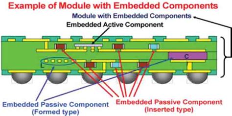
Active/Passive Component Integration Techniques
When implementing PCB manufacturing strategies for embedded systems, integrating active components (like microcontrollers or sensors) and passive elements (resistors, capacitors) directly into the substrate requires precision. Leading PCB manufacturing companies employ laser-drilled microvias and sequential lamination to embed these components, minimizing signal path lengths and reducing parasitic effects by up to 40%. This approach not only enhances circuit density but also lowers PCB manufacturing cost by eliminating redundant interconnects and external wiring.
By strategically placing components during the PCB manufacturing business workflow, you achieve better thermal dissipation—critical for high-frequency applications. For example, embedding power regulators near heat-generating ICs allows direct heat transfer through the substrate, bypassing traditional thermal interfaces. Advanced firms now use hybrid materials (e.g., ceramic-filled resins) to balance CTE mismatch while maintaining signal integrity.
However, component selection impacts scalability. Smaller passives (01005 or 0201 packages) enable tighter integration but demand stricter process controls, influencing overall PCB manufacturing cost. The shift toward 3D stacking further refines this balance, as embedded designs reduce layer counts by 15–25% compared to conventional boards. This integration philosophy aligns with next-gen applications demanding compact, high-performance solutions—a core focus for modern PCB manufacturing companies.
Optimizing Performance via 3D PCB Integration
By adopting 3D PCB integration, you unlock opportunities to consolidate circuit layers while minimizing signal path lengths, directly addressing performance bottlenecks in high-frequency applications. This approach leverages vertical stacking of active/passive components within the substrate, reducing PCB manufacturing cost by eliminating redundant interconnects and shrinking board footprint. Leading PCB manufacturing companies achieve up to 40% faster signal transmission by embedding components like capacitors or resistors between dielectric layers, which lowers parasitic inductance and capacitance.
However, transitioning to 3D designs requires balancing thermal dissipation needs with layer density. Advanced PCB manufacturing processes now incorporate micro-vias and thermally conductive fillers to prevent hotspots, ensuring reliability without compromising miniaturization goals. For businesses evaluating PCB manufacturing business models, 3D integration offers a competitive edge in applications like IoT sensors or aerospace systems, where space constraints and signal integrity are critical.
When implementing this technology, prioritize collaboration with manufacturers skilled in multilayer lamination and precision alignment. Their expertise ensures that design complexities don’t escalate PCB manufacturing cost unexpectedly, while maintaining adherence to performance specifications. By optimizing both electrical and structural parameters, 3D integration transforms how modern circuits achieve efficiency without sacrificing scalability.
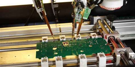
Advanced Embedded PCB Manufacturing Processes
When selecting PCB manufacturing partners for embedded designs, you need to prioritize companies specializing in sequential lamination and laser-drilled microvias. Modern PCB manufacturing companies employ additive processes like aerosol jet printing to embed components directly into dielectric layers, eliminating traditional solder joints that introduce parasitic inductance. This approach reduces PCB manufacturing cost by minimizing post-assembly rework while improving signal integrity through shorter interconnects.
The process begins with 3D substrate modeling to map component placement within multilayer stacks, followed by precision laser ablation to create cavities for active/passive elements. Advanced PCB manufacturing business operations use automated optical inspection (AOI) systems to verify embedding depths within ±15µm tolerances, ensuring consistent thermal dissipation pathways. For high-frequency applications, manufacturers integrate low-loss dielectrics (Dk < 3.5) with embedded planar inductors, achieving impedance matching directly within the board structure.
Transitioning to these methods requires reevaluating design rules—embedded copper pillars replace through-hole vias, while conformal shielding layers are deposited before final lamination. By aligning these innovations with your product’s performance targets, you can leverage embedded PCB technology to overcome spatial constraints without compromising reliability in mission-critical systems.
Embedded vs Traditional PCBs: Key Differences
When comparing embedded PCB manufacturing to traditional methods, the structural approach defines their performance gaps. Unlike conventional designs where components sit on the board, embedded PCBs integrate active/passive elements within the substrate layers. This 3D architecture minimizes parasitic effects—like inductance and capacitance—by shortening signal paths, a critical advantage for high-frequency applications.
Thermal management also diverges sharply. Traditional PCB manufacturing companies often rely on external heat sinks or fans, while embedded designs dissipate heat through the substrate itself. This reduces hotspots and improves reliability, especially in compact devices. However, PCB manufacturing cost rises with embedded systems due to complex layering and precision requirements.
For businesses, the choice hinges on application needs. While traditional PCB manufacturing business models prioritize affordability for simpler electronics, embedded solutions deliver performance gains in aerospace, medical devices, or 5G infrastructure. Transitioning requires evaluating signal integrity demands against budget constraints, as embedded processes demand advanced materials and specialized expertise. By understanding these trade-offs, you can align your project’s priorities with the right manufacturing strategy.
Future Trends in Embedded PCB Component Design
As PCB manufacturing evolves, you’ll notice a shift toward multi-functional integration in embedded designs. Leading PCB manufacturing companies are prioritizing heterogeneous integration—stacking active/passive components within 3D substrates to minimize signal loss while maximizing space efficiency. This approach not only reduces PCB manufacturing cost by consolidating materials but also aligns with demands for compact, high-performance devices.
Emerging nano-material coatings and flexible substrates are redefining thermal and electrical performance, enabling designs to withstand higher power densities. For your PCB manufacturing business, adopting AI-driven simulation tools will become critical to predicting parasitic effects early in the design phase, cutting prototyping cycles by up to 40%. Additionally, sustainable practices—like recyclable substrates—are gaining traction, balancing performance with environmental compliance.
You’ll also see tighter collaboration between chipset developers and PCB manufacturing teams to co-optimize component placement and substrate architecture. This synergy ensures that embedded interconnects and power delivery networks work seamlessly, future-proofing designs against evolving IoT and 5G requirements. By integrating these trends, you can stay ahead in a market where speed, precision, and scalability define success.
Conclusion
When evaluating PCB manufacturing solutions for advanced electronics, embedded integration proves critical for overcoming modern design challenges. By working with specialized PCB manufacturing companies, you gain access to 3D substrate technologies that minimize parasitic effects while improving thermal dissipation—key factors in high-frequency or power-intensive applications. While PCB manufacturing cost may initially appear higher for embedded designs, the long-term benefits of compact layouts, reduced component count, and enhanced reliability often justify the investment.
For businesses scaling their PCB manufacturing business, adopting embedded techniques positions you to meet evolving demands for miniaturization and signal integrity. However, success hinges on selecting partners with expertise in active/passive component embedding and multilayer substrate fabrication. As industries push toward smarter, denser electronics, prioritizing embedded PCB manufacturing ensures your designs remain competitive through optimized performance and future-ready architectures.
FAQs
How does embedded PCB integration affect overall pcb manufacturing cost?
Embedded PCB manufacturing typically involves higher upfront costs due to specialized materials and 3D substrate fabrication. However, pcb manufacturing companies often offset this through reduced assembly steps and improved long-term reliability, lowering total lifecycle expenses.
What distinguishes pcb manufacturing business strategies for embedded vs. traditional PCBs?
PCB manufacturing for embedded designs prioritizes precision layer stacking and thermal simulation tools, requiring tighter collaboration between design and production teams. This contrasts with traditional workflows focused on surface-mounted component optimization.
Can smaller enterprises afford embedded PCB solutions?
Yes. Many pcb manufacturing companies now offer scalable 3D integration services, allowing you to phase in embedded components for critical circuit blocks while managing pcb manufacturing cost through modular design approaches.
How do parasitic effect reductions impact performance metrics?
By embedding passive components within substrates, pcb manufacturing minimizes trace inductance/capacitance, enabling higher signal integrity thresholds. This is particularly valuable for RF and high-speed digital applications outlined in your design goals.
What qualifications should you prioritize when selecting a partner?
Look for pcb manufacturing business providers with ISO 9001-certified processes, proven expertise in HDI (High-Density Interconnect) substrates, and thermal stress-testing capabilities to ensure reliable embedded system performance.
Ready to Optimize Your Embedded PCB Project?
For tailored solutions that balance pcb manufacturing cost with advanced performance requirements, please click here to consult with specialists in 3D substrate integration and component embedding technologies.