Optimizing Digital PCB Designs for Enhanced Performance
Key Takeaways
When considering the optimization of digital PCB designs, it is crucial to account for several key factors that can significantly impact performance. Understanding the specific requirements in pcb manufacturing will allow you to tailor your designs effectively, serving your overall project goals. Selecting the right pcb manufacturing companies can streamline production and ensure that high-quality materials are used, which is vital for maintaining signal integrity. Additionally, a deep dive into the estimated pcb manufacturing cost will enable you to balance budget constraints with design ambitions while ensuring efficient use of resources.
Focusing on techniques to enhance performance means employing strategies that minimize electrical noise and improve the reliability of signal transmission. You can utilize various design tools and software tailored for digital environments, making it easier to visualize complex multi-layer layouts and address any potential issues early in the design process. Ultimately, working closely with experts in the pcb manufacturing business will not only help you understand the nuances of production but also guide you through implementing best practices that elevate your PCB designs to new heights. For further details on seamless manufacturing processes, visit Andwin.
Introduction to Digital PCB Design
In today’s fast-paced electronic landscape, the art of digital PCB design has become increasingly vital for achieving high-performance electronic products. As you venture into the realm of pcb manufacturing, it is essential to grasp the fundamental principles that govern effective designs. One of the cornerstones of this understanding is recognizing the importance of signal integrity, which pertains to maintaining the quality and reliability of electrical signals as they traverse through your multilayer layouts. In doing so, collaborating with reputable pcb manufacturing companies can lead to significant enhancements in the performance and efficiency of your designs.
When optimizing your digital PCBs, consider factors such as layer stack-up, trace width, and spacing, which can dramatically influence electrical performance. Initiating an effective design process begins with proper planning that seamlessly integrates these considerations into your layout. Often overlooked is the impact specific features may have on overall system performance. For instance, poorly executed decisions during layout could increase your pcb manufacturing costs due to prototype revisions or even production delays.
To streamline this process further, adopting robust design tools and methodologies can be invaluable in achieving a successful outcome. By leveraging advanced simulation software that accounts for factors like crosstalk and electromagnetic interference, you equip yourself with insights necessary for making informed decisions. Remember, your choices in design can significantly influence not only the quality but also the sustainability of your pcb manufacturing business.
"Investing time in understanding signal integrity fundamentals can save you considerable costs down the line."
Focusing on these pivotal aspects right from the initial stages will pave the way for optimized digital PCB designs that hold up under real-world conditions while minimizing unexpected challenges during production.
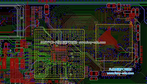
Key Considerations for Multi-Layer Layouts
When engaging in pcb manufacturing, particularly for digital PCB designs, understanding the nuances of multi-layer layouts is crucial for maximizing performance and reliability. One of the most significant challenges you may encounter is ensuring adequate spacing between signals to minimize crosstalk and maintain signal integrity. This can be achieved by carefully planning your layer stack-up and considering the placement of ground planes. Using advanced routing techniques can greatly reduce interference, which is essential for high-speed applications.
Furthermore, the pcb manufacturing cost can be influenced by your design choices; ensuring a compact and efficient layout can lead to savings in materials and production time. Collaborating with reputable pcb manufacturing companies that offer modern tools can provide insights into effective design practices, enabling you to optimize both performance and cost-effectiveness in your pcb manufacturing business. Additionally, always consider thermal management while designing your multi-layer PCB; implementing proper ventilation paths between layers will prevent overheating, which could compromise the integrity of your components.
By integrating these key considerations into your design approach, you will not only enhance the overall performance of your digital PCBs but also create a more efficient and economical manufacturing process in today’s competitive marketplace.
Techniques for Enhancing Signal Integrity
In the realm of digital PCB design, enhancing signal integrity is crucial for ensuring reliable performance in your circuits. You should first focus on the layout of your printed circuit board (PCB), as the arrangement of traces can significantly affect how signals propagate. Implementing controlled impedance strips can help maintain consistent resistance and minimize reflections during signal transmission. Additionally, it’s essential to keep your traces as short as possible while considering the pcb manufacturing process; this minimizes inductance and capacitance, which could lead to signal degradation.
Another effective technique is the strategic use of ground planes. By providing a low-impedance path for return currents, they reduce electromagnetic interference, thereby bolstering overall signal quality. When working with multiple layers, ensure there’s a sufficient separation between power and signal layers to prevent any interference caused by high-frequency signals.
Furthermore, incorporating via stitching can significantly improve return paths by connecting ground layers throughout your design. This method not only enhances signal integrity but also aids in thermal management in more complex designs. As you navigate options with various pcb manufacturing companies, keep in mind that implementing these techniques may influence the overall pcb manufacturing cost, but they are invaluable in achieving optimal circuit performance.
Remember that simulation tools can play a pivotal role during the design phase. By using software to predict how changes will affect signal behavior before committing to prototype fabrication through the pcb manufacturing business, you can save time and resources while enhancing your PCB’s reliability and effectiveness.
Strategies for Reducing Electrical Noise
When designing digital PCBs, one significant challenge arises from electrical noise, which can compromise the performance of your circuit. To effectively tackle this issue, it is crucial to implement a combination of techniques. First, you should consider the layout of your traces; keeping them as short and direct as possible can help minimize inductance and capacitance, which are critical in reducing noise. Additionally, maintaining adequate spacing between signal and ground layers is essential for enhancing the overall signal integrity of your design. Using differential pairs for your signal traces can also mitigate common-mode noise effects. Furthermore, you may want to strategically place decoupling capacitors near power pins to provide a local reservoir of energy, stabilizing voltage levels and reducing fluctuations caused by transient loads. Engaging with reliable pcb manufacturing companies can ensure that the manufacturing process aligns with your design’s unique specifications and that the pcb manufacturing cost remains within budget while maintaining quality. Keeping in mind the challenges presented by electrical noise will help you enhance performance dramatically during subsequent stages of your pcb manufacturing business. By prioritizing these strategies throughout design development, you are likely to achieve superior functionality in your digital PCB designs.
Power Distribution in Digital PCBs
Effective power distribution in digital PCBs is crucial for maintaining device reliability and optimizing performance. When designing, you should ensure that the power delivery network (PDN) is robust enough to handle varying loads without introducing significant voltage drops. This involves careful layout considerations to minimize impedance and reduce noise. A well-designed PDN requires using multiple layers, as available in multi-layer layouts, which supports efficient routing of power and ground planes. When selecting components, consider their voltage and current ratings, as well as the pcb manufacturing cost, which may vary based on the complexity and materials used. You can increase efficiency by utilizing via stitching techniques to connect different layers effectively, leading to a more stable power distribution throughout your circuit. Additionally, collaborating with reputable pcb manufacturing companies can provide valuable insights into material selection and fabrication techniques that enhance your design’s integrity. By prioritizing these strategies in your PCB design process, you can mitigate issues related to electromagnetic interference (EMI) while ensuring that your digital circuit operates at peak performance. Understanding the nuances of your pcb manufacturing business can further enhance the quality and reliability of your designs, ultimately leading to successful implementation in end products. By achieving an optimal balance between power integrity and performance characteristics, you ensure that your digital PCBs meet the demands of modern electronics effectively.
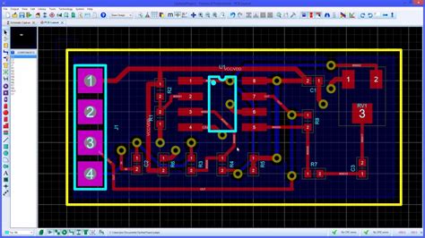
Design Tools and Software for Optimization
When it comes to optimizing your digital PCB designs, utilizing the right design tools and software can make a significant difference in both performance and efficiency. With an ever-increasing demand for tighter tolerances and higher frequencies, you must choose tools that not only streamline your workflow but also enhance your designs’ reliability. Many PCB design applications offer advanced features such as signal integrity analysis, thermal simulation, and real-time DRC (Design Rule Checks) that ensure your layout adheres to the stringent requirements of modern circuits.
Moreover, leveraging software solutions that focus on design for manufacturability is crucial when working with pcb manufacturing companies. Such tools can help you evaluate the pcb manufacturing cost from an early stage, allowing you to make informed decisions about materials and processes. Features that simulate standard manufacturing processes enable you to anticipate issues that could arise during production, thereby reducing risks associated with costly revisions later on.
As a designer, focusing on user-friendly interfaces can also significantly enhance your efficiency. Various design programs come equipped with drag-and-drop functionalities and customizable libraries that facilitate quick modifications. Understanding the intricacies of different pcb manufacturing businesses could also aid in choosing software best suited for your specific PCB types, as some applications specialize in certain sectors.
Finally, don’t underestimate the value of collaboration features embedded in modern design environments. Sharing designs with team members or external partners can result in constructive feedback early in the design phase, minimizing errors and optimizing performance before reaching production.
Testing and Validation of Digital PCB Designs
Testing and validation are crucial steps in the development of digital PCBs, ensuring that designs meet specified performance criteria and operate reliably in real-world conditions. As a designer, you should be proactive in implementing various testing methods throughout the design process. Initially, simulation tools can be invaluable for identifying potential issues in your layout before the physical prototype is produced. Utilizing software that specializes in signal integrity and thermal analysis will allow you to predict performance under different operational scenarios.
Once prototypes are available, conducting thorough physical tests is essential to validate your assumptions. This includes functional testing, where you ensure the circuitry operates as intended, and stress testing to simulate extreme conditions that the PCB may encounter. It’s vital to measure parameters like voltage levels, current flow, and signal quality. With insights gained from these tests, adjustments can be made to the design for optimization.
Moreover, collaboration with PCB manufacturing companies can lead to deeper insights into common manufacturing issues that could affect your design’s performance. They may provide feedback on the feasibility of certain structures within your layout or suggest materials that could mitigate issues like electrical noise. Understanding how your designs translate into actual production can often help refine your final version before moving forward with volume production.
Additionally, keep an eye on the pcb manufacturing cost since complexity often drives up expenses; balancing performance enhancements with cost-effectiveness is vital for maintaining competitiveness in a crowded market. With careful testing and iterative improvements based on collective feedback from both simulations and physical trials, you can optimize your digital PCB design for superior functionality while mitigating potential risks associated with production delays or failures. The results will empower you to develop robust digital PCBs that perform reliably across a range of applications while keeping overall costs manageable within your pcb manufacturing business strategy.
Future Trends in Digital PCB Technology
As the electronics industry continues to evolve, the ## Future Trends in Digital PCB Technology are set to transform how you approach pcb manufacturing. One of the significant trends is the integration of advanced materials that enhance thermal management and signal integrity. You can expect to see an increase in pcb manufacturing companies focusing on eco-friendly and efficient materials, making your designs not only more effective but also more sustainable. Moreover, advancements in automation and AI-driven design tools are streamlining pcb manufacturing costs, allowing for quicker turnaround times and reduced errors in your designs. Innovations such as 3D printing techniques are also beginning to disrupt traditional methods, providing you with the flexibility to rapidly prototype and test new designs at a lower cost. As you navigate this dynamic landscape, keeping an eye on these trends will be crucial for maintaining a competitive edge in your pcb manufacturing business, as they will directly impact both the performance of your products and your bottom line. Embracing these innovations not only positions you for success but also aligns with the ongoing push for smarter and more efficient technologies across all sectors of electronics.
Conclusion
In the realm of pcb manufacturing, it’s paramount to recognize how enhancements in digital PCB design directly influence the overall performance of electronic devices. By integrating effective strategies such as scrutinizing layer counts, optimizing trace widths, and ensuring proper grounding techniques, you can significantly improve signal integrity. Moreover, partnering with leading pcb manufacturing companies can provide valuable insights into quality materials and advanced manufacturing processes that further reduce the pcb manufacturing cost while enhancing performance. It’s also beneficial to stay ahead of industry trends to ensure your designs are compatible with emerging technologies, which can help your pcb manufacturing business thrive in an increasingly competitive market. Remember, a well-optimized digital PCB not only meets functional requirements but also fosters greater reliability and efficiency in its applications.
FAQs
What is digital PCB design?
Digital PCB design refers to the process of creating printed circuit boards specifically tailored for digital circuits. It involves the use of computer-aided design (CAD) software to layout components and interconnections, ensuring efficiency in pcb manufacturing.
How can I optimize performance in my digital PCB?
To optimize performance in your digital PCB, focus on enhancing signal integrity, reducing electrical noise, and utilizing proper power distribution techniques. Choosing reliable pcb manufacturing companies that understand these principles can significantly improve your outcomes.
What are the key considerations for multi-layer PCBs?
When designing multi-layer PCBs, consider factors such as layer stack-up, routing strategies, and grounding techniques. Effective collaboration with pcb manufacturing partners can help you manage costs while ensuring high-quality results.
How does electrical noise impact PCB performance?
Electrical noise can degrade signal quality and lead to malfunctioning circuits. By implementing noise reduction techniques during your design process, you can enhance overall performance and reliability in your digital PCBs.
What should I keep in mind regarding the cost of PCB manufacturing?
The pcb manufacturing cost can vary significantly based on material selection, complexity of the design, and volume. Planning ahead and working with experienced manufacturers will help you stay within budget while maximizing quality.


