Optimizing EGS002 Inverter Layouts for High-Power Applications

Key Takeaways
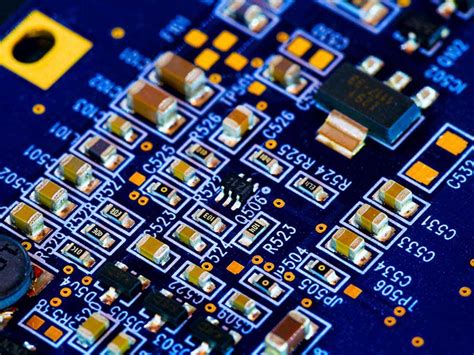
When designing high-power EGS002 inverters, prioritizing PCB manufacturing fundamentals ensures reliability at 1kW+ outputs. Start by evaluating PCB manufacturing cost trade-offs: thicker copper layers (2-4 oz) improve current handling but require collaboration with PCB manufacturing companies specializing in high-current designs. For thermal management, integrate copper pours as heat sinks while maintaining signal integrity—this reduces hotspots without compromising PCB manufacturing business viability.
Leverage 4-layer stackups to isolate high-frequency SPWM signals from power planes, a strategy refined by experienced PCB manufacturing partners. When selecting components, balance efficiency and cost by opting for MOSFETs with low RDS(on) and drivers matched to EGS002’s timing requirements. For EMI reduction, use star grounding and minimize loop areas in high-current paths—a critical consideration often overlooked in budget-focused PCB manufacturing workflows.
Always validate designs through efficiency testing under full load, using infrared imaging to identify thermal bottlenecks early. By aligning layout decisions with PCB manufacturing capabilities, you ensure scalability from prototyping to mass production without sacrificing performance.
High-Power EGS002 Inverter Fundamentals
When designing high-power inverters (1kW+) with the EGS002 module, understanding core electrical principles becomes critical. Voltage spikes and current density directly impact reliability, requiring precise coordination between the driver board and power stage. For optimal performance, you’ll need to collaborate with experienced PCB manufacturing companies to balance PCB manufacturing cost with material quality—a key consideration for high-current paths exceeding 30A.
Here’s a comparison of critical parameters for 1kW+ designs:
| Parameter | Standard Design | Optimized EGS002 Layout |
|---|---|---|
| Trace Width (Power) | 4mm | 6-8mm |
| Thermal Resistance | 2.5°C/W | 1.2°C/W |
| Switching Loss | 18% | 9-11% |
Proper PCB manufacturing prioritizes thick copper layers (https://www.andwinpcba.com). Remember: inadequate cooling in high-power scenarios can reduce MOSFET lifespan by up to 70%, making material selection as vital as circuit topology.
As you scale beyond 1kW, parasitic inductance in busbars and DC links becomes a dominant efficiency constraint. This demands meticulous component positioning—keep high-frequency switching elements (IGBTs/MOSFETs) within 5cm of the EGS002 driver outputs to prevent timing mismatches. Balancing these factors ensures your design meets both performance targets and commercial viability in competitive PCB manufacturing markets.
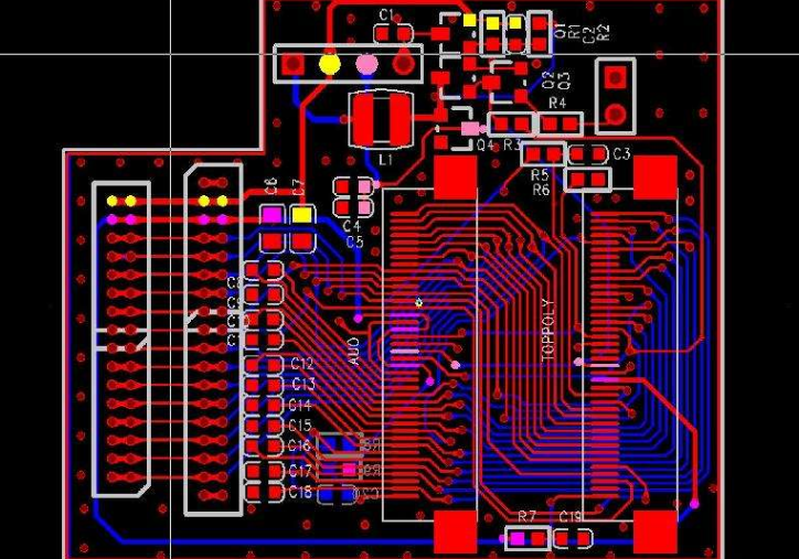
PCB Layout Strategies for 1kW Systems
When designing PCB layouts for 1kW inverters using the EGS002 module, prioritizing high-current trace routing is non-negotiable. Start by allocating 70-100 mil trace widths for power paths to minimize resistive losses, and use star grounding to prevent noise coupling. Work closely with PCB manufacturing companies to confirm copper weight (2 oz minimum) and layer stackup compatibility, as these directly impact PCB manufacturing cost and thermal performance.
Tip: Calculate trace temperature rise using IPC-2152 standards—oversized traces may reduce efficiency gains by increasing parasitic capacitance.
Place MOSFETs and diodes symmetrically near the EGS002 driver to shorten gate drive paths, ensuring precise SPWM integration. Separate analog and power grounds with a split-plane strategy, connecting them only at the DC bus capacitor. For thermal management, integrate thermal vias under high-heat components and coordinate with your PCB manufacturing partner to validate heat dissipation capabilities during prototyping.
When optimizing for PCB manufacturing business scalability, standardize component footprints to simplify assembly. Avoid 90-degree angles in high-current traces—45-degree bends reduce electromagnetic interference (EMI) risks. Double-check clearance and creepage distances, particularly in 230VAC sections, to meet safety standards.
Pro Insight: Use polygon pours for power rails, but keep them isolated from sensitive control signals to prevent voltage spikes from disrupting SPWM timing.
By balancing these strategies, you’ll achieve a layout that withstands 1kW demands while maintaining alignment with PCB manufacturing cost targets and reliability requirements.
Advanced Thermal Management Techniques
When designing high-power inverters using the EGS002 platform, effective thermal management becomes critical for sustained 1kW+ operation. Start by optimizing PCB manufacturing choices: select substrates with high thermal conductivity, such as aluminum-backed or ceramic-filled laminates, which PCB manufacturing companies often reserve for power electronics. Strategically place thermal vias beneath high-current components like MOSFETs or IGBTs to channel heat toward ground planes or external heatsinks.
For designs exceeding 500W, active cooling integration is non-negotiable. Pair your layout with temperature-controlled fans or liquid cooling channels, ensuring airflow paths align with component hotspots. When collaborating with PCB manufacturing business partners, verify their capability to handle heavy copper traces (2-4 oz), which reduce resistive losses and distribute heat more evenly.
Monitor PCB manufacturing cost trade-offs—thicker copper layers and advanced thermal materials increase expenses but prevent costly failures in high-demand scenarios. Use thermal simulation tools during prototyping to validate heat dissipation patterns, adjusting component spacing or heatsink placement as needed. Finally, ensure all thermal interfaces (e.g., thermal pads or epoxy) comply with the inverter’s operating temperature range, as even minor mismatches can degrade efficiency over time. By balancing material selection, layout precision, and collaboration with experienced PCB manufacturing specialists, you create systems that withstand rigorous thermal stress while maintaining peak performance.
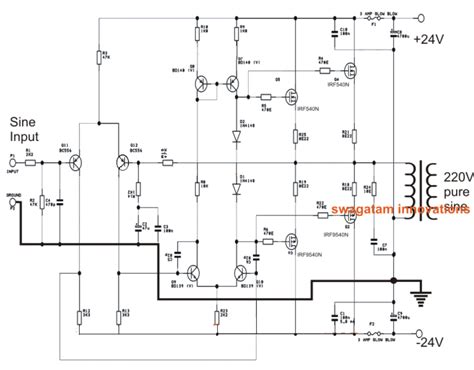
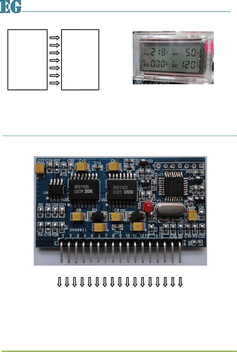
SPWM Integration in High-Current Designs
When integrating SPWM (Sinusoidal Pulse Width Modulation) into high-current inverter designs, balancing signal precision with power handling becomes critical. For systems exceeding 1kW, you’ll need to optimize gate driver placement to minimize parasitic inductance while maintaining clean switching transitions. Prioritize PCB manufacturing techniques like 4-layer stackups to isolate control and power planes, reducing electromagnetic interference (EMI) risks inherent in high-frequency SPWM operation.
Collaborating with experienced PCB manufacturing companies ensures proper trace width calculations for high-current paths, particularly when dealing with 100A+ peaks. Use thermal relief patterns around MOSFETs and IGBTs to manage heat dissipation without compromising solder joint reliability—a common oversight in high-density layouts. To control PCB manufacturing cost, consider hybrid designs that combine thick copper layers (2oz+) for power stages with standard layers for control circuitry.
For stable SPWM performance, maintain <1% voltage ripple by placing decoupling capacitors within 15mm of switching devices. Verify timing synchronization between multiple SPWM channels using impedance-matched traces, a feature advanced PCB manufacturing business partners can achieve through controlled dielectric materials. Remember: even minor impedance mismatches in high-current loops can degrade waveform fidelity, leading to inefficient power conversion at 1kW+ loads.
Component Selection for 1000W Inverters
When selecting components for 1kW inverter systems, you must balance performance, durability, and PCB manufacturing cost efficiency. Start with high-current MOSFETs rated for at least 100V/150A to handle continuous power surges, ensuring minimal switching losses. Pair these with low-ESR electrolytic capacitors (2000μF+) to stabilize voltage ripple under heavy loads. For magnetics, use toroidal cores with litz wire to reduce eddy current losses—critical for maintaining efficiency in high-power designs.
Thermal management begins at the component level: opt for thermally enhanced packages and integrate copper pours on the PCB for heat dissipation. PCB manufacturing companies often recommend 2oz copper layers for power traces, which lowers resistance and improves current handling. When sourcing parts, prioritize vendors specializing in PCB manufacturing business solutions, as they provide components pre-validated for thermal and electrical stress.
Don’t overlook auxiliary circuits—gate drivers must match MOSFET switching speeds, and current sensors should offer ±1% accuracy. For PCB manufacturing, specify high-Tg FR-4 substrates to withstand elevated operating temperatures. While balancing performance and PCB manufacturing cost, avoid undersizing connectors or using thin traces, which risk premature failure in 1kW+ applications. Remember that component choices directly impact EMI and efficiency, aligning with broader system goals covered in later sections.
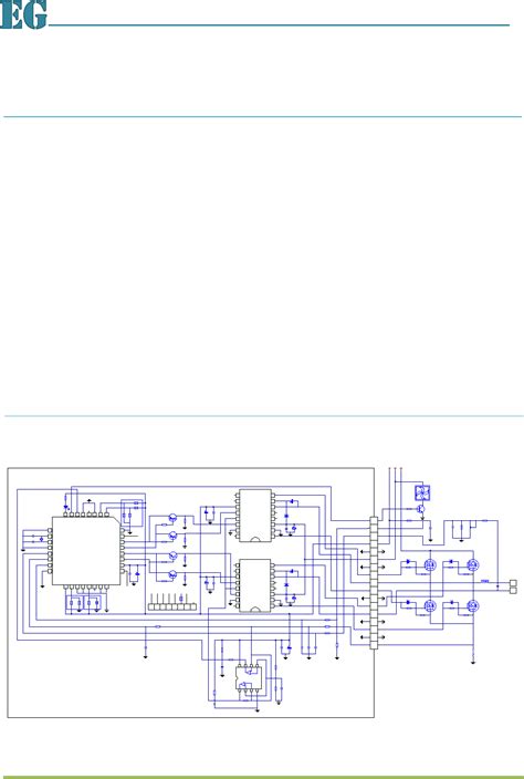
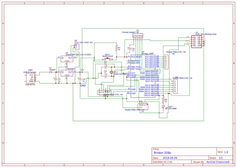
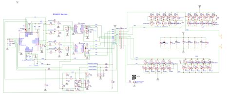
EGS002 Board Stackup Optimization Methods
When designing PCB manufacturing solutions for high-power EGS002 inverters, your board stackup configuration directly impacts thermal performance, signal integrity, and long-term reliability. Start by selecting a symmetrical layer arrangement to minimize warpage during assembly—critical for maintaining consistent thermal management in 1kW+ systems. For example, a 4-layer design with power planes sandwiched between signal layers reduces electromagnetic interference (EMI) while providing low-impedance paths for high-current traces.
Prioritize dielectric materials with high glass transition temperatures (Tg >170°C) to withstand prolonged heat stress, especially when collaborating with PCB manufacturing companies specializing in power electronics. Copper weight matters: 2-oz outer layers handle current surges, while 1-oz inner layers balance PCB manufacturing cost without compromising conductivity. Ensure prepreg thickness aligns with voltage isolation requirements—thinner cores improve heat dissipation but require precise fabrication tolerances.
When optimizing for SPWM integration, separate analog and digital ground planes to prevent noise coupling. Use via stitching around high-current components to enhance thermal relief and mechanical stability, a practice often overlooked in standard PCB manufacturing business workflows. Finally, validate your stackup with impedance simulations to avoid costly redesigns, ensuring your EGS002 layout achieves both electrical efficiency and manufacturability.
EMI Reduction in High-Power Inverter Layouts
When designing EGS002-based inverters for 1kW+ applications, managing electromagnetic interference (EMI) becomes critical to ensure stable operation and compliance with regulatory standards. Start by collaborating with experienced PCB manufacturing companies to implement multi-layer stackups with dedicated ground planes—this reduces loop areas and minimizes radiated noise. Position high-current traces (like those carrying SPWM signals) away from sensitive control circuits, and use guard traces or shielding where necessary.
For PCB manufacturing cost optimization, balance copper thickness and trace spacing: thicker copper lowers resistance but increases parasitic capacitance. Integrate snubber circuits near switching components like MOSFETs to dampen voltage spikes, and place decoupling capacitors as close as possible to IC power pins. When planning your PCB manufacturing business strategy, consider using EMI filters at input/output terminals, which add minimal material cost while significantly reducing conducted emissions.
Always validate your layout with near-field probes during prototyping, focusing on switching nodes and transformer regions. Proper grounding—star-point configurations for analog/digital domains and thermal vias for heat dissipation—ensures both EMI control and compatibility with earlier thermal management strategies. By addressing these factors early in the design phase, you’ll achieve compliance with FCC/CE standards while maintaining the efficiency gains outlined in previous sections.
Efficiency Testing Protocols for 1kW Output
When validating PCB manufacturing designs for 1kW EGS002 inverters, you’ll need structured protocols to ensure consistent efficiency under load. Start by measuring input-to-output power ratios at incremental loads (20%–100%) using calibrated digital meters. For thermal validation, infrared imaging of MOSFETs and transformer junctions helps identify hotspots exceeding 85°C—a critical threshold for PCB manufacturing cost optimization.
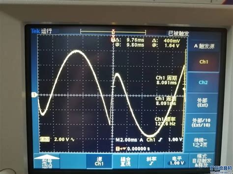
Collaborate with PCB manufacturing companies to integrate high-current test points directly into the board layout, enabling real-time voltage drop analysis. Load banks with adjustable power factors (0.7–1.0) simulate real-world conditions, while oscilloscopes track SPWM waveform integrity at peak currents. Ripple voltage should stay below 3% of the nominal output to avoid efficiency losses.
For long-term reliability, conduct 48-hour stress tests at 80% load, monitoring component derating and PCB manufacturing business viability. Document efficiency curves to compare design iterations, focusing on reducing conduction losses in traces and vias. Always verify that your testing environment aligns with IEC 62040-3 standards to ensure compliance and repeatability across production batches.
Conclusion
When finalizing your EGS002 inverter layout for high-power applications, collaboration with experienced PCB manufacturing companies becomes critical. The interplay between PCB manufacturing cost and performance demands careful balancing—opting for thicker copper layers (2 oz+) improves current handling but may increase production expenses. To maintain competitiveness in the PCB manufacturing business, prioritize designs that minimize complex via patterns while ensuring optimal heat dissipation through strategic component placement.
Your thermal management strategy should align with PCB manufacturing capabilities, as improper material selection (e.g., FR-4 vs. high-Tg substrates) can compromise long-term reliability in 1kW+ systems. Always validate SPWM timing and gate driver placement through prototyping, leveraging manufacturer feedback to refine trace widths and isolation gaps. Remember, efficiency gains in high-power inverters hinge on harmonizing electrical performance with manufacturable layouts—test iteratively with your fabrication partner to strike this balance. By integrating these principles, you’ll achieve robust designs that meet both technical and economic requirements for industrial-scale applications.
FAQs
What’s the optimal PCB thickness for 1kW EGS002 inverters?
For high-current designs, use PCB manufacturing with 2oz copper layers and 1.6mm substrate thickness. This balances thermal performance and structural integrity, especially when partnering with PCB manufacturing companies specializing in power electronics.
How does component placement affect thermal management?
Position MOSFETs and diodes near board edges for easier heatsink integration. Group high-heat components on one side to simplify cooling solutions – a critical consideration when calculating PCB manufacturing cost for multi-layer designs.
Can standard FR-4 material handle 1kW+ applications?
While FR-4 works for low-to-mid power, consider high-Tg laminates for sustained 1kW operation. Reputable PCB manufacturing business providers often recommend Isola IS410 or Rogers materials for improved thermal stability.
What’s the cost difference between 2-layer and 4-layer layouts?
Four-layer boards increase PCB manufacturing cost by 30-50%, but provide dedicated power planes that reduce EMI. For EGS002 systems exceeding 800W, this becomes a necessary investment in reliability.
How do you verify layout efficiency before production?
Run thermal simulations using IR camera data from prototype testing. Many PCB manufacturing companies now offer pre-production analysis services to detect hotspots and current imbalance issues early.
Need Professional PCB Solutions for Your High-Power Inverter?
For custom EGS002 board fabrication with optimized thermal characteristics, please click here to explore industrial-grade PCB manufacturing services tailored for power electronics applications.