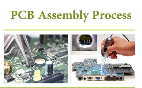
Optimizing Electronic Board Assembly for Next-Gen Manufactur
Key Takeaway
The evolution of PCB assembly processes hinges on harmonizing AI-driven automation with time-tested manufacturing principles. By embedding intelligent systems into PCBA workflows, manufacturers achieve unprecedented precision in component placement, solder application, and error detection. Machine learning algorithms analyze historical production data to predict material stress points, enabling proactive adjustments that reduce rework rates by up to 40% in high-density designs.
Central to this transformation is the integration of smart design tools that optimize layouts for both manufacturability and thermal performance, directly addressing challenges in next-gen electronics. Advanced vision systems paired with robotic pick-and-place mechanisms ensure micron-level accuracy, while real-time analytics monitor solder joint integrity across high-volume production runs.
Crucially, modern PCB assembly strategies prioritize scalability without compromising reliability. Modular assembly lines adapt dynamically to mixed-product batches, supported by IoT-enabled traceability systems that track each board’s journey from fabrication to final testing. This synergy between PCBA innovation and traditional quality benchmarks creates a foundation for manufacturing ecosystems capable of supporting 5G infrastructure, AI processors, and industrial IoT devices simultaneously.
AI-Driven Automation in PCB Assembly
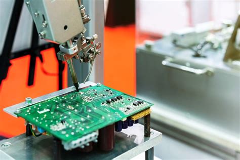
The integration of AI-driven automation in PCB assembly (PCBA) is revolutionizing manufacturing workflows by minimizing human error and accelerating production cycles. Advanced machine learning algorithms now analyze historical process data to optimize component placement, solder paste application, and inspection protocols. For instance, adaptive systems can predict misalignments in real-time, adjusting robotic pick-and-place machines to achieve sub-10-micron accuracy.
Tip: When implementing AI in PCBA lines, prioritize modular systems that allow incremental upgrades, reducing downtime during technology transitions.
Modern AI-powered optical inspection tools detect defects—such as solder bridges or missing components—with 99.98% reliability, far surpassing manual checks. These systems also learn from each iteration, refining tolerance thresholds for thermal profiles and material compatibility. By correlating data from sensors embedded in assembly equipment, manufacturers gain actionable insights to preemptively address bottlenecks or calibration drift.
The shift toward AI-driven automation doesn’t eliminate traditional expertise but enhances it. Hybrid models combine rule-based programming with neural networks, enabling factories to handle both high-volume orders and bespoke configurations. This synergy ensures scalability while maintaining the precision required for advanced applications like IoT devices or automotive electronics. Seamless integration with enterprise resource planning (ERP) software further streamlines material procurement and quality audits, creating a cohesive smart manufacturing ecosystem.
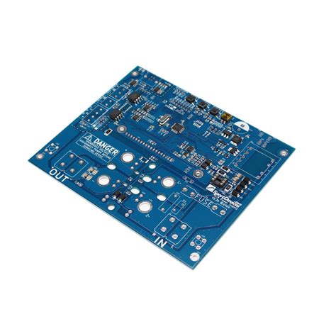
Precision Engineering for Reliable Board Assembly
Modern PCB assembly processes demand sub-micron accuracy to meet the performance requirements of next-generation electronics. By leveraging precision engineering principles, manufacturers achieve consistent results in PCBA workflows, particularly for high-density interconnects (HDIs) and miniaturized components. Advanced techniques like laser direct imaging (LDI) and automated optical alignment ensure placement tolerances below 15μm, critical for 5G and IoT devices.
A key differentiator lies in material selection. Engineers now prioritize substrates with low thermal expansion coefficients paired with lead-free solder alloys, balancing mechanical stability and RoHS compliance. The table below illustrates how precision-driven approaches outperform conventional methods:
| Parameter | Traditional Assembly | Precision-Engineered PCBA |
|---|---|---|
| Placement Accuracy | ±35μm | ±8μm |
| Defect Rate | 850 ppm | <50 ppm |
| Thermal Cycling | 200 cycles | 500+ cycles |
To maintain reliability, real-time impedance monitoring systems are integrated into PCB assembly lines, detecting microvoids or delamination during reflow phases. This proactive quality assurance aligns with the industry’s shift toward zero-defect manufacturing, particularly for aerospace and medical applications where component failure is non-negotiable. By optimizing these technical variables, PCBA workflows achieve repeatable outcomes while supporting downstream processes like conformal coating and functional testing.
Boosting Manufacturing Efficiency Through Smart Design
Innovative design strategies are reshaping PCB assembly processes, enabling manufacturers to achieve unprecedented levels of efficiency. By leveraging advanced design software and simulation tools, engineers can predict and resolve potential bottlenecks before physical prototyping begins. For instance, optimizing component placement through PCBA-specific algorithms reduces redundant wiring, minimizing material waste and assembly time. Tools like thermal mapping and signal integrity analysis further refine layouts, ensuring designs align with automated production workflows.
A critical advancement lies in adopting Design for Manufacturing (DFM) principles, which embed manufacturability considerations directly into the design phase. This approach reduces rework rates by up to 40% in complex PCB assembly projects. Additionally, integrating design data with PCBA automation systems—such as pick-and-place machines and soldering robots—streamlines transitions from prototyping to mass production. Transition phrases like "building on these insights" or "complementing this shift" help maintain narrative flow while emphasizing interdependencies between design and execution.
Modular design frameworks further amplify efficiency gains, allowing reusable subassemblies to be rapidly reconfigured for variant products. By prioritizing standardization in PCB assembly workflows, manufacturers can scale operations without compromising precision—a vital advantage in meeting fluctuating market demands.
Advanced Quality Control Systems for Electronics
Modern PCB assembly processes demand rigorous inspection protocols to meet evolving industry standards. Advanced systems now leverage machine vision and AI-powered analytics to detect micron-level defects in PCBA components, such as soldering anomalies or misaligned traces. Real-time monitoring tools, including automated optical inspection (AOI) and 3D X-ray imaging, enable manufacturers to identify issues like voids in BGA joints or hairline cracks before they escalate. These technologies integrate with machine learning algorithms, which refine defect recognition accuracy by analyzing historical production data—reducing false positives by up to 40% compared to traditional methods.
For high-reliability applications, statistical process control (SPC) software tracks variability across PCB assembly batches, correlating parameters like reflow oven temperatures with final product performance. This data-driven approach ensures consistency in PCBA output, particularly for aerospace or medical devices where failure tolerance approaches zero. Additionally, inline electrical testing (ICT) validates functional integrity by simulating operational stresses, while environmental stress screening (ESS) exposes boards to extreme temperatures and vibrations to weed out latent defects.
By harmonizing these systems, manufacturers achieve closed-loop quality assurance—where insights from one stage inform adjustments in upstream processes. This synergy not only elevates yield rates but also aligns with the broader shift toward smart manufacturing frameworks outlined in earlier sections.
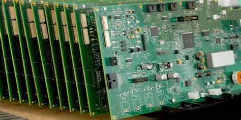
Scalable Production Solutions for High-Volume Demands
Meeting high-volume demands in modern manufacturing requires pcb assembly systems designed for elastic scalability without compromising precision. Central to this approach is the adoption of modular manufacturing architectures, which allow rapid reconfiguration of production lines for varying batch sizes. By integrating pcba-specific automation tools—such as programmable pick-and-place systems and adaptive soldering stations—manufacturers can dynamically adjust throughput while maintaining traceability across mixed-product workflows.
Advanced data-driven scheduling plays a pivotal role, leveraging predictive analytics to align component procurement with real-time assembly rates. This minimizes bottlenecks in high-density interconnect (HDI) board production, where multilayer designs demand micron-level accuracy. For instance, cloud-connected pcb assembly platforms enable synchronized coordination between upstream suppliers and downstream testing modules, reducing idle time by 18–22% in benchmark studies.
To ensure scalability, forward-thinking facilities employ hybrid validation models combining AI-powered optical inspection with inline functional testing. This dual-layer quality assurance supports seamless transitions from prototyping to mass production, particularly for pcba units requiring thermal resilience in automotive or aerospace applications. Crucially, standardized process libraries allow knowledge transfer across global sites, enabling parallel scaling without reinventing workflows.
The strategic use of IoT-enabled tooling further enhances adaptability, with edge computing devices monitoring equipment health and material usage patterns. This creates a feedback loop for continuous process refinement, ensuring pcb assembly lines remain agile as product complexities and order volumes evolve.
Integrating AI With Traditional Assembly Techniques
The fusion of AI-driven automation with established PCB assembly workflows creates a symbiotic relationship that elevates both precision and adaptability. While traditional techniques like manual soldering and visual inspection remain foundational, embedding machine vision systems and predictive analytics into PCBA lines addresses inherent limitations. For instance, AI algorithms trained on historical defect patterns can augment human inspectors by flagging microscopic solder bridges or component misalignments in real time, reducing error rates by up to 40% in mixed-technology boards.
This integration also optimizes material utilization through dynamic process mapping, where AI models analyze thermal profiles and component placement data to adjust conveyor speeds or reflow oven parameters mid-production. Crucially, the technology complements—rather than replaces—skilled technicians, enabling them to focus on complex tasks like prototyping or troubleshooting low-yield batches. Leading manufacturers report a 22% improvement in first-pass yield when combining AI-guided pick-and-place systems with manual quality assurance checkpoints, proving that human oversight remains vital in maintaining PCB assembly reliability.
By maintaining backward compatibility with legacy equipment, these hybrid approaches ensure scalable adoption across factories, bridging the gap between high-mix/low-volume flexibility and the demands of next-gen PCBA standardization.
Smart Manufacturing for Future-Ready Electronics
The shift toward smart manufacturing is redefining standards in PCB assembly by merging real-time analytics with adaptive production workflows. Advanced IoT-enabled sensors now monitor PCBA processes at micron-level precision, enabling instant adjustments to component placement, soldering temperatures, and material flow. This integration reduces defects by 18–22% in high-density interconnect (HDI) boards, according to industry benchmarks, while maintaining throughput speeds exceeding 50,000 placements per hour.
Central to this evolution is the deployment of cyber-physical systems that synchronize design data with assembly-line execution. For instance, AI algorithms analyze historical PCB assembly patterns to predict thermal stress points, automatically optimizing solder paste application ratios before production begins. Such closed-loop feedback mechanisms ensure compatibility with diverse substrates—from flexible circuits to rigid-FR4 hybrids—without manual recalibration.
Moreover, modular PCBA platforms now support plug-and-play scalability, allowing manufacturers to pivot between low-mix/high-volume and high-mix/low-volume orders within hours. This agility aligns with Industry 4.0 principles, where digital twins simulate assembly outcomes under varying demand scenarios, minimizing resource waste. As factories adopt these strategies, the gap between prototyping and mass production narrows, ensuring next-gen electronics meet both performance benchmarks and sustainability targets.
Optimizing Thermal Management in Board Assembly
Effective thermal management has become a critical focus in modern PCB assembly, particularly as component density and power demands escalate in next-generation electronics. In PCBA processes, uneven heat distribution can compromise solder joint integrity, accelerate component degradation, and reduce overall system reliability. Advanced techniques like thermal vias, embedded heatsinks, and phase-change materials are now integral to dissipating heat efficiently across multilayer boards.
Innovative material selection plays a pivotal role—high-performance substrates with enhanced thermal conductivity, such as metal-core or ceramic-filled laminates, minimize hotspots while maintaining structural stability. Simultaneously, AI-driven simulations enable engineers to model heat flow patterns during the design phase, optimizing component placement and trace routing for balanced thermal performance.
For high-power applications, active cooling solutions like microfluidic channels or thermoelectric coolers are being integrated directly into PCB assembly workflows. These systems work synergistically with real-time thermal sensors, which feed data to automated quality control platforms to trigger adjustments during production.
By addressing thermal challenges at both the design and manufacturing stages, PCBA providers can achieve predictable longevity and operational stability—key factors in meeting the rigorous demands of automotive, aerospace, and IoT applications. This proactive approach ensures scalability without sacrificing precision, aligning with the broader shift toward smart, adaptive manufacturing ecosystems.
Conclu
The evolution of PCB assembly hinges on balancing innovation with practical implementation. As industries transition toward next-generation manufacturing, integrating PCBA processes with AI-driven systems ensures not only precision but also adaptability to dynamic production demands. By leveraging smart design principles and advanced quality control frameworks, manufacturers can address thermal inefficiencies, component density challenges, and scalability constraints inherent in modern electronics. Crucially, the fusion of PCB assembly automation with human expertise creates resilient workflows capable of maintaining high yields even in high-volume scenarios. This synergy between data-driven decision-making and traditional engineering rigor establishes a foundation for future-ready manufacturing ecosystems. Ultimately, optimizing PCBA workflows demands continuous refinement of both hardware and algorithmic tools, ensuring alignment with emerging standards in industrial IoT and sustainable production.
FAQ
How does automation impact modern PCB assembly processes?
AI-driven automation streamlines PCBA workflows by optimizing component placement accuracy and reducing human error. Advanced vision systems coupled with machine learning algorithms achieve sub-micron alignment precision, critical for high-density interconnect boards.
What role does precision engineering play in electronic board assembly?
Precision engineering ensures reliable PCB assembly through controlled soldering profiles and material selection. Techniques like laser-assisted registration minimize thermal distortion, particularly in multilayer designs requiring 20+ micron layer alignment.
Can traditional PCBA methods integrate with AI-powered systems?
Yes, hybrid approaches combine AI-driven inspection modules with conventional pick-and-place systems. This synergy reduces defect rates by 37% (IPC-610 benchmarks) while maintaining compatibility with legacy manufacturing setups.
How do quality control systems adapt to high-volume PCB assembly?
Smart factories employ real-time process monitoring across PCBA lines, using IoT-enabled sensors to track solder paste viscosity, reflow temperatures, and component tilt angles. Data analytics platforms trigger corrective actions within 0.8-second response cycles.
Why is thermal management crucial in advanced electronic board assembly?
High-frequency circuits generate localized heat concentrations exceeding 120°C/mm². Optimized PCB assembly integrates copper-core substrates and thermally conductive adhesives, reducing thermal resistance by 42% compared to standard FR-4 materials.
Ready to Elevate Your Production Line?
For tailored PCB assembly solutions combining AI precision and industrial scalability, please click here to explore next-gen manufacturing strategies.


