Optimizing EMS PCB Processes for Advanced Electronics Production

Key Takeaways
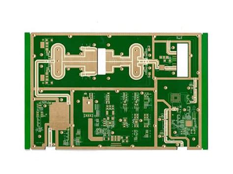
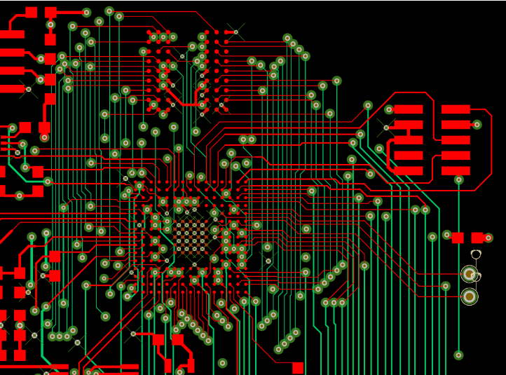
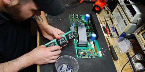
Modern PCB assembly processes demand meticulous attention to workflow optimization to meet the precision requirements of advanced electronics. Central to this is integrating PCBA (Printed Circuit Board Assembly) automation, which reduces human error and accelerates throughput. For instance, real-time monitoring systems paired with IoT-enabled devices enable manufacturers to track component placement accuracy down to micron-level tolerances.
| Traditional Approach | Optimized Strategy |
|---|---|
| Manual inspection cycles | Automated optical inspection (AOI) |
| Linear production lines | Modular, flexible workflows |
| Reactive quality checks | Predictive analytics-driven QC |
By leveraging PCBA automation tools like pick-and-place robots and AI-driven solder paste inspection, manufacturers can achieve sub-10µm alignment precision. Additionally, embedding IoT sensors in PCB assembly lines allows for continuous data collection, enabling predictive maintenance and reducing downtime by up to 30%. For deeper insights into selecting an EMS partner aligned with these strategies, explore this resource.
Transitioning to these advanced methodologies not only enhances yield rates but also ensures compliance with evolving industry standards, creating a foundation for scalable, high-reliability production.
Streamlining EMS PCB Manufacturing Workflows
Efficient PCB assembly workflows form the backbone of modern electronics manufacturing services (EMS), directly impacting production timelines and product reliability. By adopting lean manufacturing principles, EMS providers can eliminate bottlenecks in PCBA processes, such as redundant solder paste inspections or manual component placement delays. For instance, integrating automated optical inspection (AOI) systems reduces human error by 40–60% while maintaining throughput speeds above 1,200 components per hour.
Tip: Prioritize real-time data synchronization between pick-and-place machines and inventory management systems to prevent material shortages during high-volume PCB assembly.
Advanced workflow optimization also hinges on standardized design for manufacturability (DFM) guidelines, ensuring seamless transitions from prototyping to mass production. Modular production lines, configured for rapid reconfiguration between PCBA batches, cut downtime by 30% in multi-product environments. Additionally, machine learning algorithms analyzing historical process data can predict equipment maintenance needs, reducing unplanned stoppages by up to 25%.
A balanced approach combining automated traceability systems and adaptive process controls ensures consistent quality across varying production scales. For example, embedding RFID tags in panelized boards enables granular tracking from solder paste application to final testing, aligning with Industry 4.0 benchmarks. Such strategies not only accelerate cycle times but also strengthen compliance with ISO 9001 and IPC-A-610 standards, critical for aerospace and medical device sectors requiring zero-defect PCB assembly outcomes.
Enhancing PCB Assembly Precision Techniques
Achieving micron-level accuracy in PCB assembly requires a systematic approach combining advanced equipment, material science, and process optimization. Modern surface-mount technology (SMT) lines now integrate AOI (Automated Optical Inspection) systems to detect solder joint defects as small as 10μm, reducing rework rates by up to 40%. For complex high-density interconnect (HDI) designs, laser-direct imaging ensures precise alignment of PCBA components, particularly for micro-BGA and QFN packages.
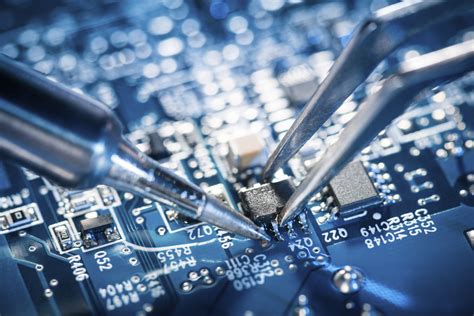
Critical to precision is the calibration of pick-and-place machinery, where vacuum nozzle configurations and vision-guided placement algorithms minimize positional deviations below ±25μm. Temperature-controlled soldering profiles, combined with nitrogen-reflow environments, further enhance solder joint consistency. Leading EMS providers like Vexos employ statistical process control (SPC) to monitor variables such as paste volume and thermal gradients in real time, ensuring adherence to IPC-A-610 standards.
Emerging techniques like 3D SPI (Solder Paste Inspection) and adaptive stencil designs address challenges in miniaturized assemblies, while machine learning models predict component drift during thermal cycling. These innovations not only refine PCB assembly accuracy but also create seamless transitions to downstream IoT-enabled quality assurance systems.
IoT Integration in Electronics Production Systems
The adoption of IoT (Internet of Things) in PCB assembly workflows is revolutionizing how manufacturers achieve precision and scalability. By embedding smart sensors across PCBA production lines, real-time data on component placement, solder quality, and environmental conditions can be monitored continuously. For instance, IoT-enabled devices track thermal profiles during reflow soldering, automatically adjusting parameters to prevent defects like cold joints or tombstoning. This granular visibility not only enhances assembly precision but also enables predictive maintenance, reducing downtime by flagging equipment anomalies before failures occur.
Advanced systems integrate IoT with machine learning algorithms to analyze historical PCBA performance data, optimizing cycle times and material usage. A practical application includes automated optical inspection (AOI) systems that share defect patterns with centralized platforms, enabling rapid corrective actions across multiple facilities. Companies like MicroArt Services leverage such interconnected frameworks to deliver high-reliability electronics manufacturing, where IoT-driven analytics align PCB assembly outcomes with stringent quality benchmarks.
As IoT networks expand, their role in synchronizing design-for-manufacturability feedback loops grows critical. Real-time collaboration between design teams and assembly floors ensures faster iterations, minimizing rework and accelerating time-to-market. This seamless integration positions IoT as a cornerstone for next-generation electronics production systems, bridging gaps between automation, quality assurance, and adaptive manufacturing strategies.
Automation Strategies for Efficient PCB Assembly
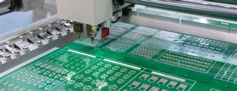
Modern PCB assembly workflows demand precision-driven automation to meet evolving industry standards. By implementing robotic pick-and-place systems, manufacturers achieve micron-level accuracy in component placement, reducing human error and accelerating throughput. These systems integrate seamlessly with PCBA inspection tools, such as automated optical inspection (AOI) and X-ray testing, enabling real-time defect detection during high-speed production.
A critical advancement lies in adaptive process control, where machine learning algorithms optimize solder paste application and reflow profiles based on component types or board geometries. This dynamic adjustment minimizes rework rates while maintaining PCB assembly consistency across mixed-product batches. For example, closed-loop feedback mechanisms adjust conveyor speeds or thermal zones to align with IoT-generated performance data, ensuring alignment with broader smart factory ecosystems.
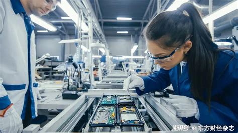
Transitioning to modular automation platforms further enhances flexibility, particularly for high-mix, low-volume production. Collaborative robots (cobots) work alongside technicians for tasks like delicate IC handling or connector alignment, merging human expertise with machine efficiency. Simultaneously, automated material handling systems (AMHS) streamline component logistics, reducing idle time between PCBA stages by 30–40%.
To maintain coherence with downstream processes, enterprises are adopting unified software architectures that synchronize PCB assembly data with enterprise resource planning (ERP) and manufacturing execution systems (MES). This integration enables predictive maintenance alerts and demand-responsive line reconfigurations, solidifying automation as the backbone of scalable electronics manufacturing.
Advanced Quality Control in EMS PCB Processes
Modern PCB assembly workflows demand rigorous inspection protocols to address the complexities of high-density interconnects and miniaturized components. Advanced quality control systems now leverage automated optical inspection (AOI) and X-ray imaging to detect microscopic defects in PCBA layers, such as solder bridging or component misalignment. These tools achieve sub-micron accuracy, ensuring compliance with aerospace and medical-grade reliability standards.
Integration of IoT-enabled sensors within production lines enables real-time monitoring of critical parameters like solder paste viscosity and reflow oven temperature profiles. By correlating this data with historical performance metrics, manufacturers can implement predictive analytics to preemptively adjust PCB assembly parameters, reducing rework rates by up to 30%. Additionally, machine learning algorithms analyze PCBA test results to identify patterns in failure modes, enabling continuous refinement of design-for-manufacturability (DFM) guidelines.
For high-mix production environments, statistical process control (SPC) software tracks variability across batches, ensuring consistency even when transitioning between product lines. This is particularly vital for applications requiring ISO 13485 or IPC-A-610 Class 3 certification. By combining smart technology with traditional inspection methodologies, EMS providers achieve a balance between precision and scalability—critical for meeting evolving demands in automotive and 5G electronics sectors.
Optimizing EMS Production with Smart Technology
The integration of smart technologies into EMS PCB manufacturing is revolutionizing how electronics are produced. By leveraging IoT-enabled systems, manufacturers gain real-time visibility into PCB assembly workflows, enabling proactive adjustments to reduce bottlenecks. For instance, embedded sensors monitor parameters like temperature and humidity during PCBA stages, feeding data into analytics platforms that optimize process stability. This connectivity ensures tighter control over solder paste application and component placement, directly enhancing assembly precision.
Automation plays a pivotal role, with robotic pick-and-place systems achieving micron-level accuracy while minimizing human error. Advanced machine vision tools inspect PCBA outputs at speeds unattainable manually, flagging defects early to prevent costly rework. Additionally, AI-driven predictive maintenance schedules equipment downtime based on usage patterns, avoiding unplanned interruptions.
A critical advancement lies in adaptive manufacturing, where machine learning algorithms analyze historical PCB assembly data to refine workflows dynamically. For example, balancing line throughput based on component availability or design complexity ensures consistent output without compromising quality. These innovations not only streamline production but also align with broader goals of sustainability by reducing material waste and energy consumption.
By merging IoT, automation, and data-driven decision-making, EMS providers unlock new levels of efficiency while maintaining the rigorous standards demanded by advanced electronics markets.
Cutting-edge EMS PCB Process Optimization Methods
Modern PCB assembly optimization relies on data-driven methodologies that integrate PCBA performance analytics with real-time process adjustments. Advanced manufacturers now deploy AI-powered optical inspection systems to detect micron-level defects during PCB assembly, reducing rework rates by up to 40%. For PCBA workflows, adaptive soldering algorithms dynamically adjust temperature profiles based on component thermal mass, ensuring consistent joint integrity across mixed-technology boards.
A pivotal innovation lies in digital twin simulations, which model PCB assembly lines to predict bottlenecks and optimize machine utilization. This approach, combined with IoT-enabled traceability, allows EMS providers to correlate production variables (e.g., solder paste viscosity, pick-and-place speed) with final PCBA reliability metrics. Additionally, machine learning tools analyze historical yield data to refine stencil designs and component placement patterns, minimizing material waste while maintaining IPC Class 3 standards.
To address high-density interconnects, manufacturers are adopting laser-assisted microvia drilling and automated conformal coating systems, which enhance precision in PCB assembly for miniaturized electronics. These techniques, when paired with closed-loop feedback from inline testing stations, create a self-optimizing PCBA ecosystem capable of scaling for 5G and IoT device demands.
Boosting Efficiency in Electronics Manufacturing
Modern electronics manufacturing demands precision and speed, particularly in PCB assembly workflows. By integrating IoT-enabled monitoring systems, manufacturers gain real-time visibility into PCBA production lines, enabling proactive adjustments to reduce downtime. Automated optical inspection (AOI) tools paired with machine learning algorithms ensure defects are identified at sub-micron levels, minimizing rework cycles. For instance, optimizing solder paste application through robotic dispensers improves yield rates by up to 15% in high-density interconnect (HDI) boards.
Strategic adoption of modular assembly platforms allows rapid reconfiguration for mixed-product batches, cutting changeover time by 30–40%. Collaborative robots (cobots) further enhance throughput in surface-mount technology (SMT) stages, handling repetitive tasks while technicians focus on complex integrations. To maintain competitiveness, leading EMS providers like OES-EMS leverage digital twins to simulate PCB assembly processes, identifying bottlenecks before physical execution. This approach not only accelerates time-to-market but also aligns with evolving standards for miniaturized, high-frequency electronics.
Balancing automation with human expertise remains critical—advanced PCBA systems now incorporate AI-driven predictive maintenance, reducing equipment failures by 25%. Such innovations underscore the industry’s shift toward smart factories, where data-driven decision-making elevates both efficiency and product reliability.
Conclusion
The evolution of PCB assembly processes within electronics manufacturing services (EMS) underscores the critical role of strategic integration between automation, IoT, and data-driven quality control. As industries demand higher precision in PCBA outcomes, adopting smart manufacturing frameworks becomes essential to maintain competitiveness. By embedding real-time monitoring systems and AI-powered analytics, manufacturers can preempt defects while optimizing throughput—ensuring that cost-efficiency aligns with rigorous performance standards.
Transitioning to modular production lines further enhances adaptability, allowing rapid scaling for diverse product portfolios without compromising assembly accuracy. Equally vital is fostering collaboration between design and manufacturing teams, which bridges gaps in design-for-manufacturability (DFM) principles. This synergy not only reduces iterative delays but also elevates first-pass yield rates across PCBA stages.
Ultimately, the convergence of automated traceability systems and IoT-enabled logistics creates a seamless feedback loop, driving continuous improvement in EMS workflows. As these innovations mature, manufacturers must prioritize workforce upskilling to fully harness emerging technologies, securing sustainable growth in an increasingly dynamic electronics landscape.
FAQs
How does automation enhance precision in PCB assembly workflows?
Automation integrates robotic placement systems and real-time monitoring to minimize human error in PCBA processes. Advanced pick-and-place machines achieve component alignment within ±25μm, while AI-driven inspection tools detect microscopic defects.
What quality control measures are critical for high-density PCB assembly?
Implementing automated optical inspection (AOI) and X-ray testing ensures reliability in PCBA for complex designs. Statistical process control (SPC) software further tracks deviations, maintaining defect rates below 50ppm in optimized EMS workflows.
How does IoT improve traceability in electronics production?
IoT-enabled sensors collect data from PCB assembly lines, enabling granular tracking of component origins, process parameters, and test results. This supports compliance with ISO 9001 and automotive-grade IATF 16949 standards.
Can flexible manufacturing systems reduce lead times for PCBA?
Yes, modular production lines with quick-change tooling adapt to mixed-volume orders, cutting setup times by 40%. Digital twin simulations further validate process changes before physical implementation.
Explore Customized PCB Assembly Solutions
For tailored PCB assembly strategies aligning with your project’s technical requirements, please click here to consult our engineering team.