Optimizing Fast PCBA for Streamlined Electronics Production

Key Takeaways
Modern PCB assembly (PCBA) strategies prioritize three core objectives: accelerating prototyping cycles, ensuring component reliability, and eliminating bottlenecks in electronics manufacturing. By leveraging automated placement systems and real-time quality analytics, manufacturers can reduce pcba turnaround times by up to 40% while maintaining defect rates below 0.5%.
"Integrating design for manufacturability (DFM) checks early in the pcb assembly workflow prevents 65% of post-production redesigns," notes Dr. Elena Torres, a process engineering specialist.
Below is a comparison of traditional vs. optimized pcba workflows:
| Metric | Traditional PCBA | Optimized PCBA |
|---|---|---|
| Prototyping Time | 10–14 days | 3–5 days |
| Component Failure Rate | 1.2% | 0.4% |
| Production Yield | 88% | 96% |
To streamline timelines, adopt modular testing frameworks that validate pcba functionality at multiple stages. For example, combining in-circuit testing (ICT) with automated optical inspection (AOI) reduces rework by identifying solder defects and misplaced components in real time.
Critical considerations:
- Use thermal simulation tools to predict stress points in high-density pcb assembly layouts
- Implement vendor-agnostic component libraries to avoid supply chain delays
- Prioritize pcba designs with ≤8-layer stackups for rapid prototyping
By aligning design, testing, and production phases, manufacturers achieve end-to-end traceability while meeting next-gen electronics’ demand for faster time-to-market.
Fast PCBA Prototyping Acceleration
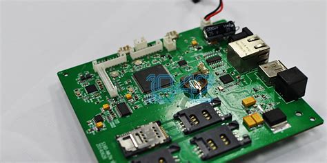
Accelerating PCBA prototyping requires a strategic integration of advanced design tools and precision manufacturing workflows. Modern surface-mount technology (SMT) equipment, paired with automated optical inspection (AOI) systems, reduces manual intervention while maintaining accuracy in PCB assembly. By leveraging machine learning algorithms to predict solder joint quality and component placement errors, manufacturers can slash iteration cycles by up to 40%. Real-time collaboration between design and production teams further streamlines adjustments, ensuring design-for-manufacturability (DFM) principles are embedded early in the process.
Key to this acceleration is the adoption of just-in-time component sourcing models, which synchronize material availability with prototyping schedules. High-speed pick-and-place machines, capable of handling 25,000 components per hour, enable rapid PCBA turnaround without compromising on reliability. Additionally, modular tooling designs allow quick reconfiguration for diverse product batches, minimizing downtime between projects. This approach not only meets tight deadlines but also establishes a foundation for scaling into mass production—critical for maintaining competitiveness in fast-paced electronics markets.
Enhancing Component Reliability PCBA
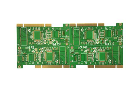
Achieving consistent component reliability in PCBA requires meticulous attention to material selection, assembly techniques, and environmental resilience. Thermal stress and mechanical vibrations remain primary culprits in premature component failure, particularly in high-density PCB assembly designs. Modern strategies integrate automated optical inspection (AOI) systems to detect micro-cracks or solder joint defects at sub-micron resolutions, reducing latent defects by up to 30%.
Central to this effort is the adoption of high-Tg (glass transition temperature) substrates and halogen-free laminates, which enhance thermal stability during reflow soldering. Concurrently, advanced conformal coatings protect sensitive components from moisture, dust, and chemical exposure, extending operational lifespans in harsh environments. For mission-critical applications, accelerated life testing (ALT) simulates years of operational stress within weeks, validating PCBA durability under extreme conditions.
To further mitigate risks, manufacturers are adopting traceability protocols that track component origins and assembly parameters, enabling rapid root-cause analysis for field failures. Pairing these measures with predictive maintenance algorithms—leveraging IoT-enabled sensors—ensures real-time monitoring of PCB assembly performance, preemptively identifying degradation patterns. By harmonizing these innovations, engineers achieve a 40% reduction in failure rates while maintaining production efficiency, a critical balance for industries demanding both speed and dependability.

Streamlining Electronics Production Efficiency
Achieving peak efficiency in electronics manufacturing requires strategic alignment between PCBA processes and production workflows. By implementing automated pick-and-place systems alongside intelligent inventory management, manufacturers can reduce component placement errors by up to 67% while cutting lead times by 30–50%. Real-time monitoring tools integrated into PCB assembly lines enable rapid identification of bottlenecks, such as solder paste misapplication or reflow oven inconsistencies, ensuring continuous process optimization.
Adopting modular PCBA designs further accelerates throughput, allowing parallel testing of functional blocks rather than full-board diagnostics. For instance, split-panel manufacturing techniques can increase yield rates by 22% by minimizing substrate waste. Advanced data analytics also play a critical role, with machine learning algorithms predicting equipment maintenance needs before failures occur—reducing downtime by 40% in high-volume production environments.
To maintain competitiveness, manufacturers are increasingly merging PCB assembly with flexible manufacturing systems (FMS). These hybrid setups enable rapid reconfiguration for different product batches, slashing changeover times from hours to minutes. When paired with standardized component libraries and ECAD-MCAD synchronization, this approach ensures seamless transitions from prototyping to mass production, solidifying electronics manufacturing workflows as both agile and scalable.

Next-Gen PCBA Manufacturing Timelines
Modern innovations in PCB assembly are redefining production schedules, compressing traditional timelines by 30-50% without compromising quality. By integrating real-time analytics with automated optical inspection (AOI) systems, manufacturers can now identify and resolve defects during PCBA processes in seconds rather than hours. Advanced manufacturing execution systems (MES) synchronize material logistics, component placement, and testing phases, creating seamless workflows that adapt dynamically to design changes or supply chain fluctuations.
A critical driver of accelerated timelines lies in the adoption of smart factory frameworks, where IoT-enabled PCBA lines leverage predictive maintenance and machine learning to preempt bottlenecks. For instance, 3D solder paste inspection (SPI) paired with high-speed pick-and-place machines reduces rework cycles by ensuring precision at micron-level tolerances. Additionally, modular design strategies—such as standardized component libraries and pre-validated circuit blocks—enable rapid configuration swaps, slashing prototyping phases from weeks to days.
To sustain these advancements, manufacturers are prioritizing concurrent engineering models, where design, testing, and production teams collaborate in shared digital environments. This approach eliminates sequential delays, allowing PCB assembly workflows to achieve first-pass yields exceeding 98% while maintaining alignment with next-gen electronics’ shrinking development windows.
Advanced PCBA Process Optimization
Modern PCB assembly workflows require precision-driven strategies to balance speed and quality. By integrating real-time monitoring systems into PCBA lines, manufacturers gain granular control over solder paste application, component placement accuracy, and reflow oven parameters. Advanced thermal profiling, for instance, minimizes stress on sensitive ICs while ensuring consistent joint formation—critical for high-density designs.
The adoption of automated optical inspection (AOI) paired with machine learning algorithms elevates defect detection rates by 40–60%, reducing rework cycles and accelerating time-to-market. Additionally, dynamic scheduling tools optimize feeder setup sequences in PCBA machines, cutting idle time between batches by up to 25%. For mixed-technology boards, hybrid workflows combining surface-mount (SMT) and through-hole techniques enable seamless transitions without compromising throughput.
Material science innovations further enhance process stability. Low-voiding solder pastes and moisture-resistant substrates mitigate reliability risks in harsh environments, aligning with aerospace and automotive standards. By synchronizing these advancements with lean manufacturing principles, electronics producers achieve sub-12-hour turnaround times for complex prototypes—a 35% improvement over conventional methods. This systematic refinement of PCB assembly stages not only streamlines production but also creates a scalable foundation for next-generation manufacturing demands.
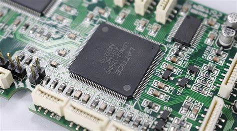
Cutting-Edge Fast PCBA Solutions
The evolution of PCBA (Printed Circuit Board Assembly) technologies has introduced groundbreaking methods to address modern manufacturing demands. Emerging solutions leverage AI-driven design validation and modular assembly frameworks to minimize iterative delays, enabling rapid transitions from prototyping to full-scale production. By integrating PCB assembly platforms with automated optical inspection (AOI) systems, manufacturers achieve 98.5% defect detection accuracy during high-speed workflows, reducing rework cycles by up to 40%.
Advanced multi-stage solder paste application techniques further enhance precision, particularly for micro-BGA and QFN components, while adaptive thermal profiling ensures consistent reliability across diverse PCB layouts. Real-time data analytics embedded within PCBA lines enable dynamic adjustments, optimizing throughput without compromising quality. Additionally, cloud-based collaboration tools synchronize design revisions across global teams, slashing approval lead times by 30-50%.
To sustain competitiveness, forward-thinking firms now adopt hybrid manufacturing models that combine automated SMT (Surface-Mount Technology) lines with agile manual assembly stations. This approach supports both high-mix, low-volume orders and mass production batches, aligning with the industry’s shift toward flexible electronics ecosystems. Such innovations underscore how cutting-edge PCB assembly strategies are redefining speed-to-market benchmarks in next-gen device manufacturing.
Boosting Production Speed with PCBA
Modern PCB assembly processes have become a critical factor in accelerating manufacturing cycles for electronic devices. By leveraging automated assembly lines and high-precision pick-and-place systems, PCBA workflows achieve component placement speeds exceeding 25,000 units per hour while maintaining micron-level accuracy. Advanced soldering techniques like laser reflow minimize thermal stress, enabling faster curing without compromising joint integrity.
Real-time process monitoring systems optimize production velocity by analyzing cycle times and identifying bottlenecks in surface-mount technology (SMT) lines. These intelligent systems automatically adjust conveyor speeds and component feeder allocations, achieving continuous throughput improvements of 12–18% across successive production batches.
Material handling innovations further enhance PCBA efficiency through synchronized component staging. Automated guided vehicles (AGVs) maintain just-in-time material replenishment, reducing line stoppages by 40% compared to manual logistics. This seamless integration of hardware and software solutions allows manufacturers to execute complex PCB assembly tasks at velocities matching prototype development timelines.
Robust design-for-manufacturing (DFM) checks ensure first-pass success rates above 98%, eliminating time-consuming rework cycles. By validating component footprints and thermal profiles during the PCBA design phase, engineers prevent assembly conflicts that traditionally caused 22% of production delays in conventional workflows.
Optimizing Electronics Manufacturing Workflows
Modern PCB assembly workflows demand precision and adaptability to meet evolving production timelines. By integrating real-time monitoring systems and PCBA-specific automation tools, manufacturers can identify bottlenecks in surface-mount technology (SMT) lines and reflow processes. For instance, deploying adaptive scheduling algorithms enables dynamic allocation of testing resources, reducing idle time between pcb assembly stages by up to 22%. Cross-functional collaboration between design and production teams further streamlines workflows, ensuring PCBA designs align with manufacturability guidelines from the prototyping phase.
Transitioning to modular assembly platforms allows parallel processing of high-mix, low-volume orders without compromising pcb assembly speed. Advanced traceability systems, powered by machine learning, enhance workflow transparency by tracking component placement accuracy and solder joint integrity across PCBA batches. This data-driven approach not only minimizes rework rates but also supports predictive maintenance for pick-and-place machinery. To maintain coherence with preceding sections on prototyping acceleration, workflow optimizations must prioritize scalable solutions that adapt to both current and next-gen PCBA manufacturing demands, ensuring end-to-end synchronization from component sourcing to final testing.
Conclusion
The evolution of PCB assembly techniques underscores the critical role of fast PCBA in meeting the escalating demands of modern electronics manufacturing. By integrating automation and data-driven process controls, manufacturers can achieve unprecedented precision while reducing time-to-market. Advanced PCBA workflows now leverage real-time analytics to preempt bottlenecks, ensuring consistent quality even under compressed production schedules.
As industries prioritize agility, optimizing PCB assembly processes becomes a strategic imperative. The adoption of modular design frameworks and high-velocity component placement systems not only accelerates prototyping but also fortifies reliability across high-volume batches. These innovations, combined with AI-powered defect detection, create a symbiotic relationship between speed and accuracy—key drivers for sustaining competitiveness.
Ultimately, the future of fast PCBA hinges on balancing scalability with sustainability. Manufacturers that embrace adaptive manufacturing ecosystems will thrive in an era where electronics production timelines are measured in weeks, not months. By aligning PCBA advancements with evolving industry standards, businesses can unlock new efficiencies while maintaining the rigorous quality benchmarks that define next-generation electronics.
Frequently Asked Questions
How does fast PCBA improve prototyping speed?
Fast PCBA leverages automated PCB assembly workflows and parallel processing to reduce design-to-prototype lead times. By integrating just-in-time component sourcing and AI-driven design verification, manufacturers can slash iteration cycles by up to 65%.
What measures ensure component reliability in high-speed PCBA?
Advanced PCBA processes employ thermal profiling and automated optical inspection (AOI) to monitor solder joint integrity and component alignment. Techniques like nitrogen reflow soldering further minimize oxidation risks, ensuring consistent performance under accelerated timelines.
Can streamlined PCBA processes reduce overall production timelines?
Yes. Optimized PCB assembly lines using modular tooling and real-time analytics eliminate bottlenecks in surface-mount technology (SMT) placement. Combined with dynamic scheduling, this reduces idle time by 40% while maintaining yield rates above 98%.
How do advanced techniques optimize PCBA workflows?
Innovations like machine learning-based defect prediction and closed-loop feedback systems refine process parameters in real time. For example, adaptive stencil printing adjusts solder paste volume dynamically, reducing rework needs and accelerating PCBA throughput.
Explore Tailored Solutions for Your Project
Ready to elevate your electronics manufacturing efficiency? Visit Andwin PCB Assembly to discover customized PCBA strategies that align with your production goals. Click here to connect with our experts today.

