Optimizing Flex PCB Layer Stack-Ups for Advanced Circuit Designs
Key Takeaways
When planning flex PCB layer stack-ups, you need to balance durability, signal integrity, and space efficiency—especially in advanced designs spanning 4-18 layers. Start by collaborating with experienced PCB manufacturing companies to validate material choices and stack-up configurations. For example, aerospace applications often require polyimide-based layers for thermal stability, while medical devices prioritize biocompatible adhesives.
"Always simulate signal paths in multi-layer flex circuits early—cross-talk increases exponentially in tightly packed designs."
Here’s a quick comparison of common layer configurations:
| Layers | Typical Use Case | Cost Impact |
|---|---|---|
| 4-6 | IoT sensors | Low |
| 8-12 | Medical imaging | Moderate |
| 14-18 | Avionics systems | High |
To minimize PCB manufacturing cost, optimize layer counts without compromising performance. Use adhesive-less substrates for thinner builds or hybrid rigid-flex designs to reduce interconnection points. Remember, PCB manufacturing business models often scale with volume—prototyping with 6-layer stacks before committing to complex 18-layer builds can save 20-30% in initial costs.
For high-frequency applications, prioritize dielectric materials with stable Dk values. Learn how material selection impacts signal loss in flex circuits. Always verify thermal expansion coefficients with your PCB manufacturing partner to prevent delamination in extreme environments.
Flex PCB Layer Stack-Up Essentials
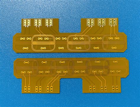
When designing flex PCB layers, balancing performance with manufacturability is critical. You’ll need to consider factors like bend radius, material thickness, and copper weight to ensure reliability in dynamic applications. For PCB manufacturing companies, the choice between single-sided, double-sided, or multi-layer configurations directly impacts PCB manufacturing cost and lead times. A typical 4-layer stack-up might include polyimide cores for flexibility and adhesive-free bonding to minimize delamination risks—a common pain point in high-reliability sectors like aerospace.
To optimize durability, staggered copper traces and symmetrical layer arrangements reduce mechanical stress during bending cycles. For signal integrity, controlled impedance layers and ground-plane shielding become essential as layer counts increase to 8 or beyond. Keep in mind that PCB manufacturing business constraints often dictate material availability, so collaborate early with suppliers to align design goals with production realities. Transitioning from rigid-flex to fully flexible designs? Prioritize thermal management and interlayer adhesion to avoid performance degradation in harsh environments. By integrating these principles, you’ll create stack-ups that meet both technical demands and cost-efficiency targets across IoT, medical, or industrial applications.
Advanced Rigid-Flex Design Techniques
When designing rigid-flex PCBs, you must balance mechanical resilience with electrical performance. Start by defining bend radius requirements early in the layout phase to prevent material stress—this directly impacts PCB manufacturing cost by reducing rework from cracked traces. For multi-layer configurations, prioritize symmetrical stack-ups to avoid warping during lamination, a common challenge in PCB manufacturing business workflows.
Collaborate closely with PCB manufacturing companies to select materials that match your application’s thermal and flex cycles. For instance, aerospace designs often require high-temperature polyimide cores, while medical devices benefit from ultra-thin adhesiveless laminates. Use controlled impedance modeling tools to maintain signal integrity across rigid-flex transitions, especially when integrating 8+ layers.
To optimize space efficiency, leverage microvias and staggered plating in high-density areas. However, remember that advanced via structures can escalate PCB manufacturing complexity—always validate feasibility through Design for Manufacturability (DFM) checks. For IoT applications, consider hybrid stack-ups combining rigid sections for components with flexible interconnects, minimizing weight without sacrificing durability.
Finally, implement dynamic flexing zones with staggered copper layers to distribute mechanical stress. This technique not only extends product lifespan but also aligns with cost-sensitive strategies in PCB manufacturing business models, ensuring reliability across harsh environments.
Optimizing Durability in Flex Circuits
When designing flex PCB layers for demanding applications, balancing mechanical resilience with performance starts with strategic material choices and structural planning. You’ll want to prioritize polyimide substrates for their heat resistance and flexibility, but pairing them with adhesive systems that maintain bond integrity during repeated bending is equally critical. For multi-layer stacks, staggered copper traces reduce stress concentration, while avoiding abrupt transitions between rigid and flex zones prevents delamination—a common failure point in PCB manufacturing.
Collaboration with experienced PCB manufacturing companies ensures alignment between design intent and production realities. For instance, specifying rolled annealed copper instead of electrodeposited variants improves fatigue resistance, directly impacting long-term durability. Advanced simulations, such as finite element analysis (FEA), help validate bend radii and layer alignment before prototyping, reducing PCB manufacturing cost by minimizing trial-and-error cycles.
In high-cycle applications like wearable medical devices, dynamic flex areas benefit from additional coverlay protection or stiffener integration at anchor points. However, over-engineering increases material waste and complicates assembly—key considerations for any PCB manufacturing business aiming to balance reliability with cost efficiency. By optimizing layer thicknesses and conductor geometries, you achieve circuits that withstand thousands of flex cycles without compromising signal paths or interlayer adhesion.
Signal Integrity for Multi-Layer Flex
Maintaining signal integrity in multi-layer flex circuits requires balancing material properties, layer arrangement, and shielding strategies. As you scale to 4-18 layer stack-ups, impedance control becomes critical—especially when high-speed signals traverse flexible sections. PCB manufacturing companies often recommend using low-dielectric substrates (like polyimide) to minimize signal loss, paired with controlled impedance traces to reduce crosstalk. For rigid-flex designs, ensure ground planes adjacent to signal layers act as reference planes, stabilizing return paths and suppressing electromagnetic interference.
To optimize PCB manufacturing cost, consider hybrid stack-ups: placing high-speed signals in rigid zones and low-frequency routing in flex areas. This reduces the need for expensive shielding films while preserving performance. However, avoid over-engineering—excessive layers or redundant shielding can inflate PCB manufacturing business expenses without tangible benefits. Advanced simulation tools help validate layer configurations before prototyping, preventing costly redesigns.
In aerospace or medical applications, where signal noise tolerance is near-zero, PCB manufacturing partners may suggest embedded passive components or differential pair routing. Always verify thermal stability and mechanical stress resistance during testing, as flexing can alter impedance characteristics over time. By aligning layer stack-up choices with application-specific demands, you ensure reliability without compromising efficiency.
Material Selection for Flex PCB Layers
Choosing the right materials for flex PCB layers directly impacts performance, durability, and PCB manufacturing cost. Start by evaluating dielectric materials like polyimide, which offers thermal stability and mechanical flexibility—critical for dynamic applications. For conductive layers, rolled annealed copper is preferred over electrodeposited variants due to its superior fatigue resistance, especially in high-bend scenarios. Adhesives matter too: acrylic-based options provide stronger bonding for multi-layer stacks but may increase rigidity, while epoxy alternatives balance flexibility and cost.
When working with PCB manufacturing companies, prioritize materials with compatible coefficients of thermal expansion (CTE) to prevent delamination during thermal cycling. For instance, pairing polyimide with low-CTE copper alloys minimizes stress in aerospace or medical devices. Don’t overlook coverlays: liquid photoimageable (LPI) solder masks enable finer pitch designs, whereas polyimide films enhance abrasion resistance.
Balancing these choices requires understanding how material trade-offs affect signal integrity and PCB manufacturing business margins. Thin substrates reduce weight but demand precise handling, raising production complexity. Collaborate closely with suppliers to align material specs with application needs—whether optimizing for IoT wearables or high-reliability industrial systems—to avoid over-engineering and unnecessary costs.
Aerospace-Grade Flex Stack-Up Solutions
When designing flex PCB layers for aerospace applications, you must prioritize solutions that withstand extreme environmental stresses while maintaining signal integrity and mechanical resilience. Aerospace-grade flex stack-ups often incorporate high-performance polyimide substrates with low CTE (coefficient of thermal expansion) to handle rapid temperature fluctuations, paired with adhesiveless copper laminates to minimize delamination risks. Collaborating with experienced PCB manufacturing companies ensures compliance with MIL-PRF-31032 or IPC-6013 standards, which mandate rigorous testing for thermal cycling, vibration resistance, and outgassing in vacuum conditions.
To optimize PCB manufacturing cost without compromising reliability, consider hybrid stack-ups combining rigid and flex layers. For instance, using 8-12 flex PCB layers with embedded stiffeners in high-stress zones reduces weight while enhancing durability—critical for avionics or satellite systems. Advanced PCB manufacturing business practices, such as laser-drilled microvias and sequential lamination, enable tighter interlayer spacing for high-frequency signal routing, essential for radar or communication modules.
Always validate designs through simulation tools to predict mechanical fatigue and thermal warpage, ensuring your stack-up aligns with mission-critical performance thresholds. By balancing material innovation and PCB manufacturing expertise, you achieve robust aerospace solutions that meet stringent size, weight, and power (SWaP) requirements.

Medical Device Flex Circuit Optimization
When optimizing flex PCB layer stack-ups for medical devices, you must balance biocompatibility requirements with high-density signal transmission needs. Implantable devices demand ultra-thin flex circuits (often 4-8 layers) that withstand repeated flexing while maintaining signal integrity in EMI-heavy environments like MRI scanners. Prioritize materials with ISO 10993-certified adhesives and low-dielectric-loss substrates to ensure both patient safety and reliable performance.
Collaborating with experienced PCB manufacturing companies becomes critical here—they’ll guide you on laser-drilled microvias for compact layouts and adhesive-less copper bonding to reduce delamination risks. For wearable diagnostics, consider asymmetric stack-ups that place rigid components near connectors while keeping sensor regions flexible. This approach minimizes PCB manufacturing costs by reducing material waste without compromising durability.
Always validate thermal management strategies early, as medical-grade flex circuits often operate in temperature-constrained environments. Advanced PCB manufacturing techniques like sequential lamination help achieve tighter impedance control for high-frequency signals in pacemakers or neural monitors. By aligning layer counts with functional requirements rather than defaulting to maximum layers, you streamline both design complexity and PCB manufacturing business timelines—key for rapid prototyping in regulated markets.
Cost-Effective Flex Layer Configurations
When balancing performance and PCB manufacturing cost in flexible circuits, strategic layer planning becomes critical. For designs requiring 4-8 layers, combining symmetrical stack-ups with polyimide-based adhesiveless materials reduces material waste while maintaining thermal stability. You’ll find that PCB manufacturing companies often recommend minimizing blind/buried vias in cost-sensitive projects—opting instead for staggered microvias to lower drilling complexity.
To optimize PCB manufacturing business margins, consider standardizing dielectric thicknesses (e.g., 25 µm or 50 µm) across layers. This reduces tooling changes and accelerates production cycles. For rigid-flex designs, hybrid stack-ups using FR-4 stiffeners alongside flexible cores cut material expenses by up to 30% without compromising mechanical integrity.
Always validate layer counts against application demands: adding unnecessary layers inflates PCB manufacturing costs but under-layering risks signal degradation. Partner with suppliers offering design-for-manufacturability (DFM) reviews to identify cost traps like excessive coverlay openings or impractical bend ratios. By aligning your stack-up strategy with volume production capabilities, you achieve durable, high-performance flex circuits that stay within budget—whether prototyping IoT wearables or scaling medical monitoring systems.
Conclusion
When finalizing flex PCB layer stack-ups, your design choices directly impact performance across aerospace, medical, and IoT applications. Successful implementation hinges on balancing durability with signal integrity, particularly when scaling to 8-18 layers. Collaborating with experienced PCB manufacturing companies ensures precise material selection—such as polyimide films or low-loss laminates—while optimizing PCB manufacturing cost through efficient layer configurations.
For high-reliability sectors like aerospace, prioritize symmetrical stack-ups with shielding layers to mitigate EMI. In medical devices, focus on ultra-thin designs that maintain flexibility without compromising impedance control. Always validate thermal and mechanical stress thresholds with your PCB manufacturing partner, as material choices directly affect longevity in dynamic environments.
Lastly, consider scalability early: designs that minimize PCB manufacturing business complexities (like hybrid rigid-flex layouts) reduce assembly time and future iteration costs. By aligning layer optimization with production realities, you achieve space-efficient, high-performance circuits that meet both technical and budgetary demands.
FAQs
How does layer count affect signal integrity in flex PCBs?
Higher layer counts (8+) enable complex routing but require precise PCB manufacturing to maintain impedance control. You’ll need advanced adhesive systems and staggered via designs to minimize crosstalk, especially in high-frequency IoT or medical devices.
What drives PCB manufacturing cost for multi-layer flex circuits?
Costs scale with layer complexity, material grades (e.g., polyimide vs. liquid crystal polymer), and tolerance requirements. Partnering with experienced PCB manufacturing companies ensures balanced durability and cost-efficiency—critical for aerospace or wearable applications.
Can rigid-flex designs reduce PCB manufacturing business expenses?
Yes. Integrating rigid and flex zones often lowers assembly costs by eliminating connectors. However, thermal management becomes critical—opt for manufacturers specializing in hybrid stack-ups to avoid delamination risks.
How do aerospace-grade flex PCBs differ from commercial designs?
They use ultra-thin copper clads (≤12µm) and high-temp laminates to withstand extreme environments. Rigorous testing by certified PCB manufacturing providers is mandatory for MIL-SPEC compliance.
When should you prioritize space efficiency over layer count?
In wearables or implantable medical devices, aim for 4-6 layers with embedded passives. This reduces PCB manufacturing cost while maintaining signal integrity through optimized via-in-pad layouts.
Ready to Optimize Your Flex PCB Stack-Up?
For tailored solutions in advanced PCB manufacturing, please click here to consult engineers specializing in aerospace, medical, and IoT-ready rigid-flex designs.