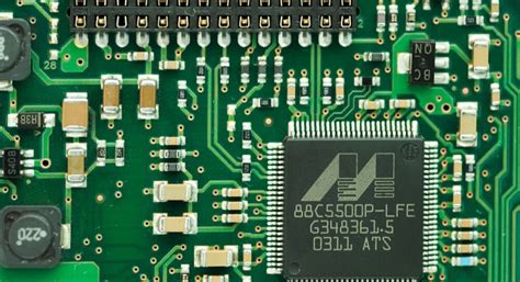
Optimizing PCB Assembly Design for Enhanced Performance
Key Takeaways
Effective PCB assembly design hinges on balancing technical precision with manufacturability At the core of PCBA optimization lies layout precision, which ensures minimal signal interference and optimal electrical performance For instance, maintaining controlled impedance traces and avoiding right-angle bends in high-frequency circuits reduces electromagnetic interference (EMI), a common pain point in dense designs
"A well-planned layout isn’t just about component placement—it’s about anticipating thermal and electrical interactions at every stage," notes a senior electronics engineer specializing in PCB assembly
Material selection further influences reliability Using substrates with high glass transition temperature (Tg) improves thermal stability, while low-loss laminates enhance signal integrity in high-speed applications For cost-sensitive projects, opting for FR-4 alternatives with balanced dielectric properties can reduce expenses without sacrificing performance
Thermal management remains critical, especially in high-density PCBA Integrating thermal vias, copper pours, and heatsinks mitigates hotspots, extending component lifespan In aerospace or automotive applications, where temperature fluctuations are extreme, combining thermal interface materials (TIMs) with strategic airflow design ensures consistent operation
To align with mass production goals, designers should adopt design for manufacturability (DFM) principles Standardizing component footprints, minimizing unique part counts, and adhering to solder mask clearance rules streamline PCBA workflows Automated optical inspection (AOI) and in-circuit testing (ICT) further validate quality, catching defects early
Pro Tip: Collaborate with your PCB assembly partner during the design phase to identify potential fabrication bottlenecks, such as oversized via pads or insufficient solder mask dams
Finally, incorporating flexible circuit elements—like rigid-flex PCBs—supports compact, lightweight designs without compromising durability This approach is particularly valuable in wearables and IoT devices, where space constraints and mechanical stress demand innovative PCBA solutions
PCB Layout Precision for Optimal Signal Integrity
Achieving optimal signal integrity in PCB assembly requires meticulous attention to trace routing, component placement, and impedance control High-speed digital circuits and analog systems demand precise layout strategies to minimize signal degradation caused by electromagnetic interference (EMI) or crosstalk A well-designed PCBA ensures critical signals follow the shortest possible paths, with controlled differential pair routing and adequate spacing between sensitive traces For example, maintaining consistent characteristic impedance across transmission lines prevents reflections, which is particularly vital in RF and high-frequency applications
Material selection directly impacts layout precision, as low-loss dielectric substrates like Rogers or Isola materials reduce signal attenuation in high-speed designs Ground plane optimization further enhances performance—strategic placement of decoupling capacitors near power pins and the use of split planes for mixed-signal circuits mitigate noise coupling Thermal considerations also play a role: uneven heat distribution can warp substrates, altering trace geometries and degrading signal paths
In PCB assembly workflows, collaboration between design and manufacturing teams ensures layout specifications align with fabrication tolerances Automated design rule checks (DRCs) verify trace widths, clearances, and via placements, while 3D modeling tools predict mechanical conflicts in multi-board systems For PCBA involving dense component arrays, microvia technology and embedded passives save space without compromising signal quality
Transitioning to advanced materials or tighter layouts must balance cost and complexity, but the long-term reliability gains justify these investments As edge-rate speeds increase in modern electronics, prioritizing layout precision during PCB assembly becomes non-negotiable for sustaining signal integrity across industrial, automotive, and consumer applications
Advanced Material Selection in PCB Assembly
The foundation of high-performance PCB assembly lies in the strategic selection of materials that balance electrical efficiency, thermal resilience, and mechanical stability Advanced material science directly impacts signal integrity, power distribution, and long-term reliability in PCBA designs For substrate materials, engineers increasingly prioritize high-frequency laminates like Rogers RO4000® series for RF applications, where low dielectric loss and stable permittivity are non-negotiable In contrast, metal-core substrates (e.g., aluminum or copper-based PCBs) are gaining traction for power electronics, offering superior heat dissipation to mitigate thermal stress in high-current scenarios
Conductive material choices extend beyond traditional copper traces Innovations such as embedded silver inks or conductive polymer pastes enable finer trace geometries in compact designs while maintaining impedance control For surface finishes, ENIG (Electroless Nickel Immersion Gold) remains a gold standard for corrosion-resistant contacts, though OSP (Organic Solderability Preservatives) is emerging as a cost-effective alternative for high-volume PCB assembly projects
The dielectric properties of solder mask materials also demand scrutiny Liquid photoimageable solder masks (LPISM) with low CTE (Coefficient of Thermal Expansion) values minimize warping during reflow cycles, particularly in multilayer PCBA configurations Additionally, thermally conductive underfill materials are critical for BGA (Ball Grid Array) components, reducing solder joint fatigue in temperature-fluctuating environments
Material compatibility with automated assembly processes cannot be overlooked For instance, halogen-free laminates align with eco-friendly manufacturing mandates but require adjusted soldering profiles to prevent delamination By correlating material datasets with DFM (Design for Manufacturability) simulations, engineers preemptively address thermal mismatches and mechanical stresses, ensuring seamless transitions to mass production This holistic approach to material selection not only elevates performance but also reduces post-assembly rework, reinforcing the economic viability of modern PCB assembly workflows
Thermal Management Solutions for High-Density PCBs
Effective thermal management is a cornerstone of reliable PCB assembly, particularly in high-density designs where component proximity amplifies heat generation As electronic devices shrink in size but grow in computational power, managing thermal loads becomes critical to preventing performance degradation, material fatigue, and premature failure
A primary strategy involves optimizing component placement to distribute heat-generating elements evenly across the board For instance, positioning high-power components like processors or voltage regulators away from thermally sensitive parts—such as MEMS sensors or precision analog circuits—reduces localized hotspots Integrating thermal vias beneath these components further dissipates heat into inner copper layers or dedicated heatsink pads In PCBA designs, combining these vias with thermally conductive epoxy or metal-core substrates (e.g., aluminum or copper) enhances heat transfer efficiency by up to 40%, as demonstrated in recent industry benchmarks
Material selection also plays a pivotal role High-temperature laminates, such as polyimide or ceramic-filled substrates, offer superior thermal stability compared to standard FR-4, maintaining structural integrity even at sustained temperatures exceeding 150°C For applications requiring extreme thermal endurance, embedded copper-invar-copper (CIC) layers or active cooling solutions—like microfluidic channels or piezoelectric fans—provide additional dissipation pathways without compromising board real estate
Advanced simulation tools are indispensable for validating thermal performance early in the design phase Computational fluid dynamics (CFD) models predict airflow patterns and temperature gradients, enabling engineers to refine heatsink geometries or adjust copper pour configurations Post-PCB assembly, infrared thermography and thermal cycling tests verify that the design meets operational thresholds, ensuring longevity in environments with fluctuating thermal conditions
Finally, aligning thermal strategies with design for manufacturability (DFM) principles ensures scalability For example, standardized heatsink mounting points or pre-tested thermal interface materials (TIMs) streamline mass production while reducing rework rates By balancing innovative cooling techniques with pragmatic PCBA workflows, designers achieve robust thermal management without inflating costs—a critical advantage in competitive electronics markets
Cost-Effective PCB Design for Mass Production
Achieving cost efficiency in PCB assembly requires balancing performance requirements with manufacturing scalability A critical starting point is optimizing component placement to minimize pcba substrate waste while maintaining signal integrity Design for Manufacturability (DFM) principles play a pivotal role here—standardizing pad sizes, avoiding overly complex via structures, and adhering to industry-standard clearance rules reduce fabrication errors and rework costs For instance, consolidating similar components into uniform orientations streamlines pick-and-place machine operations, directly lowering labor time in high-volume production
Material selection also influences cost dynamics While high-frequency laminates may suit niche applications, bulk PCB assembly workflows often prioritize FR-4 substrates with proven reliability and competitive pricing Strategic use of surface finishes—such as HASL over ENIG—can trim expenses without compromising functionality for consumer-grade electronics Additionally, panelization techniques that maximize board yield per panel, paired with breakaway tab designs, further reduce raw material waste
Thermal management strategies must align with cost goals Instead of expensive copper-filled vias, designers might opt for optimized trace routing and thermal relief patterns to dissipate heat in pcba layouts Simulation tools enable precise prediction of thermal hotspots, allowing targeted placement of lower-cost passive cooling solutions like aluminum heat sinks
Collaboration with PCB assembly partners early in the design phase ensures alignment with their equipment capabilities, preventing costly redesigns For example, designing panels compatible with a manufacturer’s depaneling machinery avoids post-production modification fees Automated optical inspection (AOI) compatibility should also guide test point placement to minimize quality control bottlenecks
Finally, supply chain resilience is integral to cost-effective mass production Standardizing component packages and qualifying alternative part suppliers mitigate risks of shortages, ensuring uninterrupted pcba manufacturing cycles By embedding these principles, engineers create designs that scale efficiently without sacrificing the robustness demanded by modern electronics markets
Improving Reliability Through Robust PCB Assembly
In modern electronics manufacturing, ensuring the long-term reliability of PCB assembly (PCBA) requires a systematic approach that addresses both design and process variables Critical factors such as component placement accuracy, soldering integrity, and material compatibility directly influence the operational lifespan of electronic devices For instance, improper solder joint formation—often caused by uneven thermal profiles during reflow—can lead to premature failure under thermal cycling or mechanical stress
A robust PCB assembly process incorporates three core strategies:
1 Advanced solder alloy selection to withstand thermal expansion mismatches
2 Automated optical inspection (AOI) systems for micron-level defect detection
3 Conformal coating applications tailored to operational environments
| Reliability Factor | Standard Practice | Advanced Solution |
|---|---|---|
| Thermal Stress Resistance | FR-4 substrates | High-Tg ceramics or polyimide |
| Vibration Resistance | Through-hole components | Surface-mount with underfill |
| Moisture Protection | Silicone conformal coatings | Parylene vapor deposition |
Transitioning from prototype to mass production demands strict adherence to IPC-A-610 standards, particularly for PCBA destined for automotive or aerospace applications Implementing design for reliability (DFR) principles early reduces field failure rates by 40-60%, according to industry benchmarks For high-density designs, thermal via arrays and copper balancing techniques prevent warpage during assembly, while trace width optimization minimizes electromigration risks in power-hungry circuits
Recent advancements in predictive maintenance algorithms now enable real-time monitoring of PCB assembly lines, correlating process parameters like solder paste volume (±002ml tolerance) with long-term reliability metrics This data-driven approach, combined with accelerated life testing (ALT) protocols, creates a closed-loop system for continuous quality improvement—a vital consideration as component miniaturization pushes traditional reliability boundaries
Design for Manufacturability in PCB Assembly Processes
Implementing Design for Manufacturability (DFM) principles in PCB assembly ensures that designs transition seamlessly from prototyping to high-volume production This approach minimizes fabrication errors, reduces rework costs, and accelerates time-to-market A critical first step involves optimizing component placement to align with automated PCBA workflows, such as pick-and-place machinery and reflow soldering systems For instance, maintaining consistent component spacing and orientation prevents misalignment during assembly, while standardized pad sizes enhance solder joint reliability
Material compatibility plays a pivotal role in DFM strategies Selecting substrates with thermal expansion coefficients that match component materials mitigates stress fractures during temperature cycling Additionally, designers must account for etching tolerances and drill hole alignment to avoid short circuits or open connections in multilayer boards Incorporating PCB assembly-specific guidelines—such as avoiding sharp angles in copper traces or providing adequate thermal relief patterns—further enhances manufacturability
Collaboration between design and manufacturing teams is essential for identifying potential bottlenecks early For example, using design rule checks (DRCs) tailored to PCBA capabilities flags issues like insufficient solder mask clearance or undersized vias Similarly, designing testability features—such as accessible test points or boundary scan compatibility—streamlines quality assurance without requiring physical probing
Balancing performance requirements with production realities ensures cost efficiency Opting for surface-mount technology (SMT) over through-hole components reduces manual labor, while standardized footprints enable bulk sourcing However, mixed-technology boards demand careful planning to avoid conflicting thermal profiles during reflow By prioritizing design simplicity and leveraging PCB assembly automation, manufacturers achieve scalable, repeatable outcomes without compromising electrical performance
Proactive thermal management integration—like strategically placing thermal vias or optimizing copper pours—supports both functionality and manufacturability These considerations, combined with adherence to industry standards such as IPC-2221, create robust designs that withstand rigorous production environments Ultimately, DFM transforms theoretical PCBA designs into manufacturable solutions, bridging the gap between innovation and industrial feasibility
Automated Testing Strategies for Enhanced PCB Performance
Implementing automated testing methodologies has become a cornerstone of modern PCB assembly processes, particularly as component densities increase and design tolerances tighten Advanced in-circuit testing (ICT) systems now leverage programmable interfaces to validate electrical connectivity across PCBA units, detecting issues like open circuits, shorts, or misplaced components with micron-level precision For high-frequency or mixed-signal boards, automated optical inspection (AOI) complements electrical tests by scanning solder joints and component alignment against pre-defined geometric benchmarks, reducing human error in quality control
To address thermal resilience in mission-critical applications, thermal cycling tests integrated into automated test equipment (ATE) simulate extreme operating conditions, ensuring PCB assembly reliability under stress Machine learning algorithms further enhance defect prediction by analyzing historical test data to identify patterns in failure modes, enabling proactive design adjustments For mass-produced PCBA units, parallel testing architectures allow simultaneous validation of multiple boards, dramatically improving throughput without compromising accuracy
Transitioning from prototype to full-scale production requires harmonizing testing protocols with design for manufacturability (DFM) principles For instance, incorporating standardized test points during layout planning ensures compatibility with automated probe systems, while minimizing redundant checks streamlines workflow efficiency As flexible circuits and embedded components gain traction, adaptive testing frameworks that combine boundary scan techniques with 3D X-ray inspection are becoming essential for verifying interlayer connections in multilayer PCB assembly designs
By aligning these strategies with the broader objectives of cost efficiency and reliability outlined in earlier sections, manufacturers can achieve a balanced approach to PCBA quality assurance—one where automated systems not only identify defects but also contribute actionable insights for iterative design refinement
Integrating Flexible Circuits in Modern PCB Designs
The adoption of flexible circuits in PCB assembly represents a paradigm shift in electronics design, enabling solutions for space-constrained and high-performance applications Unlike rigid boards, flexible printed circuits (FPCs) leverage polyimide or polyester substrates to achieve bendability while maintaining electrical integrity This innovation is particularly valuable in wearable devices, aerospace systems, and medical equipment, where PCBA designs must accommodate dynamic mechanical stress and three-dimensional packaging requirements
A critical advantage lies in reduced interconnect complexity—flexible circuits eliminate the need for bulky connectors and solder joints between multiple rigid boards This consolidation enhances signal reliability by minimizing impedance mismatches, a common challenge in high-frequency PCB assembly workflows However, designers must address unique thermal considerations: flexible substrates typically exhibit lower heat dissipation than FR-4 materials, necessitating strategic placement of thermal vias or hybrid rigid-flex configurations in PCBA layouts
Material selection also plays a pivotal role High-temperature polyimide films, paired with rolled annealed copper, provide optimal durability for repeated flexing cycles For applications requiring extreme precision, laser-drilled microvias enable denser component placement without compromising mechanical flexibility Advanced simulation tools, such as 3D electromagnetic modeling, are now indispensable for predicting stress distribution and validating bend radii before prototyping
Integration with automated PCB assembly processes demands careful planning Flexible circuits often require specialized fixtures during soldering to prevent warping, while selective stiffener placement ensures compatibility with pick-and-place machinery Manufacturers report 15–20% reductions in assembly errors when using pre-bent FPCs in automated PCBA lines, underscoring the importance of design-for-manufacturability principles
As industries push toward miniaturization and IoT connectivity, the synergy between flexible circuits and traditional PCB assembly methodologies will continue to redefine performance benchmarks Balancing mechanical resilience with electrical precision remains key to unlocking next-generation applications—from foldable displays to implantable biomedical sensors
Conclusion
The evolution of PCB assembly processes underscores the critical balance between technical precision and practical manufacturability By prioritizing signal integrity through optimized layout strategies and leveraging advanced materials, designers can address both performance and reliability challenges in high-density PCBA applications Effective thermal management remains non-negotiable, particularly as component miniaturization pushes the limits of heat dissipation in modern electronics
A forward-looking approach to PCB assembly integrates design for manufacturability (DFM) principles early in the development cycle, ensuring cost-efficiency without compromising quality The adoption of automated testing protocols further strengthens this synergy, enabling rapid validation of complex circuits while minimizing production delays For industries transitioning to mass production, the strategic use of flexible circuit integration demonstrates how adaptability in PCBA design can future-proof products against evolving technological demands
Ultimately, success in PCB assembly hinges on a holistic view that harmonizes electrical performance, mechanical robustness, and economic viability As the industry shifts toward smarter, more interconnected systems, embedding these optimization strategies will remain pivotal in achieving scalable, reliable, and high-performing electronic solutions
FAQs
How does layout precision impact signal integrity in PCB assembly?
Accurate component placement minimizes electromagnetic interference and crosstalk, ensuring stable signal transmission Advanced PCBA designs often use impedance-controlled routing and ground plane optimization to maintain high-frequency performance
What factors guide material selection for high-reliability PCB assembly?
Key considerations include thermal expansion coefficients, dielectric constants, and operating temperature ranges High-speed applications typically require low-loss laminates, while industrial environments may prioritize glass transition temperatures in PCBA substrates
Why is thermal management critical in modern PCB assembly designs?
High-density layouts generate concentrated heat fluxes that can degrade component lifespan Effective solutions combine thermal vias, heat sinks, and conductive adhesives in PCBA configurations, particularly for power electronics and RF systems
How do PCB assembly techniques affect manufacturing costs?
Standardized component footprints and panelization strategies reduce assembly time by 18-25% in mass production Design for manufacturability principles in PCBA workflows help avoid costly re-spins through proper solder mask clearances and component spacing validation
What testing protocols ensure reliability in complex PCB assembly projects?
Automated optical inspection (AOI) and in-circuit testing (ICT) verify 973% of solder joints in multilayer PCBA Environmental stress screening (ESS) further validates performance under temperature cycling and vibration loads
Can flexible circuits be integrated with traditional PCB assembly processes?
Yes, hybrid rigid-flex designs using polyimide substrates now account for 22% of advanced PCBA applications Proper bend radius calculations and strain relief features maintain durability while enabling compact form factors
Ready to Optimize Your PCB Assembly Workflow?
For tailored PCBA solutions combining precision layout design and advanced thermal management, please click here to consult our engineering team: https://wwwandwinpcb.com/pcb-assembly/