Optimizing PCB Board Assembly for Peak Performance
Key Takeaways
Optimizing PCB assembly (PCBA) requires a balance of design precision, material robustness, and process efficiency. Below are critical insights to achieve peak performance in electronics manufacturing:
- Design Optimization: Layout choices directly influence assembly efficiency. Prioritize component placement symmetry and thermal relief patterns to minimize soldering defects and signal interference.
- Advanced Techniques: Leverage automated optical inspection (AOI) and pick-and-place systems for micron-level accuracy in component positioning, reducing human error.
- Material Selection: High-performance substrates like FR-4 or polyimide ensure durability under thermal stress, while lead-free solder alloys enhance reliability.
Tip: Always validate material compatibility with operating conditions (e.g., temperature ranges, humidity) to prevent premature PCB failure.
| Factor | Traditional Approach | Advanced Approach |
|---|---|---|
| Component Placement | Manual alignment | AI-driven pick-and-place |
| Inspection | Visual checks | AOI and X-ray imaging |
| Thermal Management | Basic heat sinks | Embedded cooling channels |
- Automation Integration: Streamline workflows with smart manufacturing tools, such as IoT-enabled assembly lines, to monitor real-time metrics like solder paste viscosity and reflow oven profiles.
- Quality Assurance: Implement rigorous testing protocols, including in-circuit testing (ICT) and functional testing, to identify latent defects before deployment.
By focusing on these pillars, manufacturers can elevate PCBA outcomes, ensuring reliability and longevity in high-demand applications.
Introduction to PCB Board Assembly and Performance Optimization
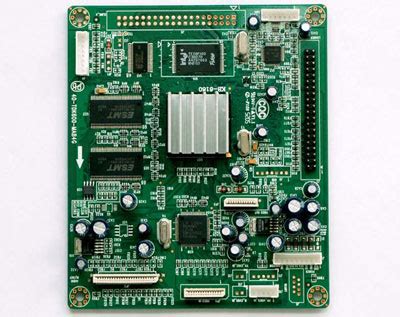
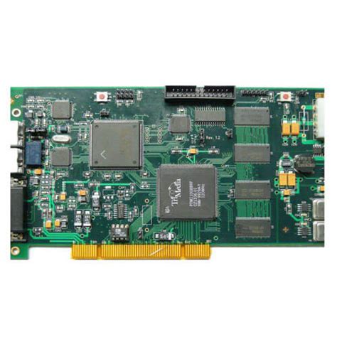
PCB assembly (often abbreviated as PCBA) forms the backbone of modern electronics, where components are meticulously mounted onto a printed circuit board to create functional systems. Achieving peak performance in PCBA requires a strategic balance of design precision, material integrity, and process efficiency. At its core, the assembly process involves soldering components—such as resistors, capacitors, and integrated circuits—onto a PCB board, ensuring electrical connectivity and mechanical stability. However, optimizing this process demands more than just technical execution; it hinges on design foresight and advanced methodologies to address challenges like signal integrity, thermal dissipation, and component density.
A critical factor in performance optimization lies in aligning PCB assembly workflows with rigorous design standards. For instance, component placement must account for signal path minimization to reduce electromagnetic interference (EMI), while material selection—such as high-temperature laminates or low-loss dielectrics—ensures reliability under demanding operating conditions. Additionally, leveraging automated optical inspection (AOI) and surface-mount technology (SMT) enhances precision during component placement, reducing human error and improving yield rates. By integrating smart manufacturing tools, such as real-time monitoring systems, manufacturers can streamline workflows and preemptively identify bottlenecks.
Ultimately, the goal is to produce PCBA solutions that deliver consistent performance across diverse applications, from consumer electronics to industrial machinery. This requires a holistic approach, where every stage—from prototyping to mass production—prioritizes quality control, thermal management, and scalability. As technology evolves, embracing innovations like embedded components and flexible PCB designs will further push the boundaries of what optimized PCB assembly can achieve.
Key Design Considerations for Efficient PCB Assembly
Designing a PCB assembly for peak performance requires balancing precision, manufacturability, and long-term reliability. A critical starting point is optimizing component placement to minimize signal interference and thermal hotspots. By strategically arranging high-power components away from sensitive analog circuits and ensuring adequate spacing, designers can reduce electromagnetic interference (EMI) and improve signal integrity. Additionally, adhering to Design for Manufacturability (DFM) principles—such as standardizing pad sizes and avoiding overly dense layouts—streamlines the PCBA process, reducing errors and rework during production.
Material selection plays a pivotal role in ensuring durability. High-quality substrates like FR-4 or polyimide, paired with robust solder masks, enhance thermal stability and resistance to environmental stressors. For high-frequency applications, materials with low dielectric loss are essential to maintain signal clarity. Thermal management must also be addressed early in the design phase, with features like thermal vias, heatsinks, or copper pours to dissipate heat efficiently and prevent component degradation.
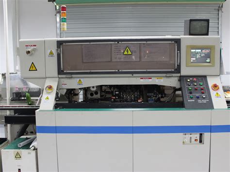
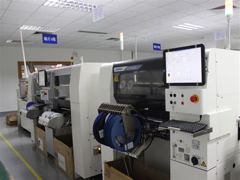
Automation is another cornerstone of efficient PCB assembly. Pick-and-place machines equipped with vision systems enable rapid, accurate placement of surface-mount devices (SMDs), while reflow ovens with precise temperature profiles ensure consistent solder joint quality. Integrating smart technology, such as IoT-enabled monitoring systems, allows real-time tracking of assembly parameters, further minimizing defects.
Finally, collaboration between design and manufacturing teams is vital. Prototyping with iterative testing helps identify potential bottlenecks, such as misaligned footprints or inadequate clearances, before full-scale production. By prioritizing these considerations, engineers can achieve a PCBA that delivers both performance and reliability, laying the foundation for advanced electronics in demanding applications.
Advanced Techniques for Precision Component Placement
Achieving precision in PCB assembly hinges on deploying advanced methodologies that minimize errors while maximizing performance. Central to this process is the use of automated pick-and-place systems, which leverage high-speed robotics and machine vision to position components with micron-level accuracy. These systems reduce human error and ensure consistent placement, even for ultra-fine-pitch or miniature components common in modern PCBA designs.
Incorporating surface-mount technology (SMT) optimizes component density, enabling compact layouts without compromising functionality. However, success relies on precise solder paste application through stencil printing, which demands meticulous control over parameters like aperture design and paste viscosity. For mixed-technology boards combining SMT and through-hole components, selective soldering systems provide targeted heat application, preventing thermal stress on sensitive parts.
Advanced PCB assembly workflows also integrate 3D automated optical inspection (AOI) to validate placement accuracy post-soldering. By comparing real-time images against design specifications, AOI systems flag misalignments, tombstoning, or solder bridging, enabling rapid corrections. Pairing this with X-ray inspection ensures hidden defects, such as voids in ball grid arrays (BGAs), are identified early.
To further enhance precision, engineers employ thermal profiling during reflow soldering. By tailoring temperature curves to specific components and materials, manufacturers avoid issues like cold joints or delamination. Additionally, laser-assisted alignment tools improve registration for multi-layer boards, ensuring vias and pads align perfectly across layers.
Material choices also play a pivotal role. Using low-voiding solder pastes and high-tg substrates minimizes mechanical stress during thermal cycling, directly impacting long-term reliability in PCBA. Combined with real-time data analytics, these techniques create a feedback loop, refining processes iteratively for peak performance.
By integrating these strategies, manufacturers achieve not only precision but also scalability, meeting the demands of high-volume PCB assembly while maintaining stringent quality standards.
Ensuring Reliability Through Robust Material Selection
The foundation of a reliable PCB assembly lies in the strategic selection of materials that withstand operational stresses while maintaining electrical and mechanical integrity. Thermal stability, chemical resistance, and mechanical durability are critical factors when choosing substrates, conductive layers, and protective coatings. For instance, high-performance PCBA often employs FR-4 or specialized laminates like polyimide for flexible circuits, which offer exceptional heat resistance and dimensional stability. Conductive materials, such as copper with electroless nickel immersion gold (ENIG) finishes, ensure low oxidation and consistent solderability, even in harsh environments.
Adhesives and encapsulants also play a pivotal role in mitigating vibration and moisture ingress. Thermal interface materials (TIMs), like silicone-based pads or epoxy resins, enhance heat dissipation in high-power applications, directly impacting PCB assembly longevity. Additionally, solder mask quality influences resistance to environmental factors—opt for liquid photoimageable (LPI) solder masks for fine-pitch components, as they provide precise coverage and robust insulation.
Material compatibility is equally vital. Mismatched coefficients of thermal expansion (CTE) between layers can lead to delamination or cracking during thermal cycling. Advanced PCBA designs often integrate low-CTE substrates paired with compatible conductive inks to minimize stress. For mission-critical applications, halogen-free materials are increasingly preferred to meet environmental and safety standards without compromising performance.
Automation in material handling further enhances reliability by reducing contamination risks. Automated dispensers apply adhesives and coatings with micron-level precision, while pick-and-place systems ensure components are mounted on optimally prepared surfaces. By prioritizing robust material selection alongside advanced PCB assembly techniques, manufacturers achieve a balance between durability, efficiency, and peak performance in modern electronics.
Streamlining Processes with Automation and Smart Technology
Modern PCB assembly workflows are increasingly leveraging automation and smart technologies to achieve unparalleled efficiency, accuracy, and scalability. By integrating advanced robotic systems, such as automated pick-and-place machines, manufacturers can drastically reduce human error while accelerating component placement speeds. These systems utilize high-resolution vision systems and machine learning algorithms to ensure micron-level precision, even when handling miniaturized or complex components. Additionally, PCBA lines now incorporate real-time monitoring through IoT-enabled sensors, which track parameters like temperature, humidity, and vibration during assembly. This data-driven approach enables proactive adjustments, minimizing downtime and ensuring consistent quality across production batches.
Another critical advancement is the adoption of automated optical inspection (AOI) systems, which perform rapid, non-destructive checks for soldering defects, misalignments, or missing components. Coupled with AI-powered analytics, these tools identify patterns in defects, allowing engineers to refine processes iteratively. For high-mix, low-volume production—common in industries like aerospace or medical devices—flexible automation platforms enable quick reconfiguration of PCB assembly lines, reducing setup times and enhancing adaptability.
Smart technology also plays a pivotal role in material handling and inventory management. Automated guided vehicles (AGVs) and RFID tracking systems streamline the movement of components, ensuring just-in-time delivery to assembly stations while reducing waste. Furthermore, digital twin simulations allow manufacturers to model and optimize PCBA workflows virtually before physical implementation, mitigating risks and accelerating time-to-market.
By harmonizing automation with intelligent data analytics, manufacturers achieve not only faster production cycles but also long-term cost savings and improved product reliability. These innovations are redefining industry standards, making PCB assembly more resilient to evolving technological demands.
Quality Control Measures for High-Performance PCB Assembly
In high-performance PCB assembly (PCBA), rigorous quality control measures are critical to ensure precision, reliability, and compliance with industry standards. The process begins with automated optical inspection (AOI), which scans assembled boards for soldering defects, component misalignment, or missing parts. This step is complemented by X-ray inspection to examine hidden connections, such as those in ball grid arrays (BGAs), ensuring solder joint integrity and void detection. For mission-critical applications, functional testing simulates real-world operating conditions to validate electrical performance, signal integrity, and thermal behavior.
Material traceability is another cornerstone of quality assurance. By verifying the authenticity and specifications of components and substrates, manufacturers mitigate risks associated with counterfeit parts or substandard materials. Advanced PCBA workflows also integrate statistical process control (SPC), leveraging real-time data analytics to monitor production trends and preemptively address deviations. Additionally, conformal coating and environmental stress testing (e.g., thermal cycling, humidity exposure) assess the board’s resilience under extreme conditions, safeguarding long-term durability.
Collaboration between design and manufacturing teams further enhances quality outcomes. Implementing design for manufacturability (DFM) principles early minimizes assembly errors, while post-production audits ensure adherence to IPC-A-610 or similar standards. By combining automated inspection tools, robust testing protocols, and proactive process optimization, PCB assembly achieves the precision required for next-generation electronics, delivering consistent performance in aerospace, automotive, and industrial applications.
Thermal Management Strategies for Enhanced PCB Longevity
Effective thermal management is critical to ensuring the longevity and reliability of PCB assembly (PCBA) in high-performance electronics. As components become smaller and power densities increase, managing heat dissipation becomes a central challenge. Excessive heat can degrade materials, warp substrates, and lead to premature component failure, directly impacting the operational lifespan of the assembly.
One foundational approach involves selecting materials with inherent thermal stability. High-temperature laminates, such as polyimide or ceramic-filled substrates, offer superior heat resistance compared to standard FR-4 boards. Additionally, integrating thermally conductive adhesives and metal-core PCBs helps channel heat away from sensitive components, reducing localized hotspots. For multilayer designs, strategically placing thermal vias—plated holes that transfer heat between layers—enhances overall thermal conductivity.
Component placement also plays a pivotal role. Positioning high-power devices like voltage regulators or processors near the board’s edges or adjacent to heat sinks improves airflow and heat dissipation. Advanced automated optical inspection (AOI) systems in modern PCBA workflows ensure precise alignment of these components, minimizing thermal stress caused by misalignment.
Another key strategy is the use of active cooling solutions, such as fans or liquid cooling systems, paired with passive methods like heat sinks or thermal pads. Simulation tools, including finite element analysis (FEA), allow engineers to model heat distribution during the design phase, optimizing layouts before prototyping. For applications requiring extreme durability, conformal coatings with high thermal resistance shield components from environmental stressors while maintaining efficient heat transfer.
Finally, rigorous testing under simulated operational conditions validates thermal management effectiveness. Techniques like infrared thermography identify hotspots, while accelerated life testing ensures the assembly withstands prolonged thermal cycles. By integrating these strategies, manufacturers achieve PCBA designs that balance performance, reliability, and longevity in demanding environments.
Future Trends in PCB Assembly for Next-Generation Electronics
The evolution of PCB assembly (PCBA) is accelerating to meet the demands of next-generation electronics, driven by advancements in miniaturization, connectivity, and sustainability. One key trend is the adoption of high-density interconnect (HDI) technology, enabling tighter component placement and reduced signal loss—critical for applications like 5G, IoT, and wearable devices. As devices shrink, embedded components and 3D-printed circuits are gaining traction, allowing for more compact designs without compromising performance.
Another emerging focus is the integration of flexible and rigid-flex PCBs, which cater to irregularly shaped devices and dynamic environments. These boards, combined with advanced automated optical inspection (AOI) systems, ensure precision in PCBA while minimizing human error. Additionally, the shift toward environmentally sustainable materials—such as halogen-free substrates and lead-free solders—reflects the industry’s commitment to reducing ecological footprints without sacrificing reliability.
Automation remains central to future-proofing PCB assembly, with AI-driven pick-and-place machines and robotic soldering systems enhancing throughput and repeatability. Machine learning algorithms are also being leveraged to predict and mitigate defects early in the production cycle. Meanwhile, the rise of smart factories equipped with IoT-enabled monitoring tools enables real-time adjustments, optimizing yield and reducing downtime.
Finally, the growing demand for high-frequency and high-speed PCBs in aerospace, automotive, and telecommunications underscores the need for advanced thermal management solutions. Innovations like liquid cooling integration and thermally conductive substrates are becoming essential to maintain performance in extreme conditions. As these trends converge, the PCBA landscape will continue to prioritize precision, adaptability, and sustainability to power the electronics of tomorrow.
Conclusion
Optimizing PCB assembly processes is critical to achieving peak performance in modern electronics. By integrating advanced design principles, precision manufacturing techniques, and rigorous quality controls, manufacturers can ensure that PCBA (printed circuit board assembly) delivers the reliability and efficiency demanded by today’s high-tech applications. A focus on thermal management—such as using high-conductivity substrates or strategic component spacing—prevents overheating and extends the lifespan of assembled boards. Additionally, leveraging automation in component placement and soldering minimizes human error while boosting production speed, ensuring consistency across large-scale batches.
Material selection also plays a pivotal role; opting for robust substrates and high-performance solders enhances durability under stress or environmental challenges. Furthermore, adopting smart technologies like AI-driven inspection systems enables real-time defect detection, reducing rework costs and improving yield rates. As industries push toward miniaturization and higher power densities, innovations such as embedded components and flexible PCBs are reshaping the future of PCBA, enabling lighter, faster, and more adaptable devices.
Ultimately, the path to optimized PCB assembly lies in balancing precision, innovation, and scalability. By staying ahead of emerging trends—such as IoT integration and sustainable manufacturing practices—companies can maintain competitiveness while meeting the evolving demands of next-generation electronics.
Frequently Asked Questions
What design considerations are critical for optimizing pcb assembly?
Key design factors include component placement, trace routing, and thermal management. Prioritizing high-speed signal integrity and minimizing electromagnetic interference (EMI) ensures efficient pcba performance. Using design-for-manufacturing (DFM) principles reduces errors and speeds up production.
How does precision component placement impact pcb assembly quality?
Advanced pick-and-place machines enable micron-level accuracy, reducing soldering defects and misalignment. Automated optical inspection (AOI) systems further validate placement, ensuring pcb assembly meets stringent tolerances for high-performance applications like aerospace or medical devices.
Why is material selection vital for reliable pcba?
Robust substrates (e.g., FR-4, polyimide) and high-quality solder alloys enhance durability under thermal stress. Selecting materials with low dielectric loss and high thermal conductivity improves signal stability and heat dissipation in pcb assembly.
Can automation improve pcb assembly efficiency?
Yes. Automated solder paste dispensing, reflow ovens, and AOI systems streamline workflows, reduce human error, and accelerate throughput. Smart factories integrate IoT-enabled analytics to predict and resolve pcba bottlenecks in real time.
What quality control measures ensure high-performance pcb assembly?
Testing methods like in-circuit testing (ICT), X-ray inspection, and functional testing validate electrical performance and structural integrity. Environmental stress screening (ESS) simulates extreme conditions to confirm pcba reliability.
How does thermal management affect pcb assembly longevity?
Effective heat dissipation through thermal vias, heatsinks, or embedded copper layers prevents component degradation. Optimizing airflow and using materials with high thermal resistance extend the lifespan of pcb assembly in high-power applications.
What trends are shaping the future of pcba?
Innovations like additive manufacturing for flexible PCBs, AI-driven defect detection, and eco-friendly materials are revolutionizing pcb assembly. Miniaturization and IoT integration demand higher precision and smarter production workflows.
Ready to Optimize Your PCB Assembly Process?
Explore advanced pcb assembly solutions tailored for your project’s needs. For expert guidance and cutting-edge pcba services, please click here to visit Andwin PCB.


