Optimizing PCB Design and Fabrication for Enhanced Performance

Key Takeaways
Optimizing PCB design and fabrication involves a comprehensive understanding of the fundamental principles and the latest techniques that can significantly enhance the performance of PCBA (Printed Circuit Board Assembly). Key aspects include the selection of appropriate materials which directly influences both performance and cost-efficiency. For instance, using high-quality substrates can improve thermal management and signal integrity, contributing to a more reliable end product. Moreover, advanced fabrication processes such as laser cut or 3D printing techniques are revolutionizing how PCBs are manufactured, allowing for intricate designs that were previously unfeasible. Incorporating simulation and testing methodologies early in the design phase is vital for identifying potential issues before they arise in the production stage. These proactive measures can lead to significant reductions in development time and associated costs. Furthermore, embracing cost-effective strategies in PCB production, such as bulk purchasing of materials or optimizing production runs, not only lowers expenses but can also enhance reliability through fewer iterations in manufacturing. As the landscape of electronics continues to evolve, staying informed about future trends in PCB design and fabrication will be critical for businesses aiming to remain competitive in a fast-paced market. The synergy between top-notch design practices and efficient fabrication techniques ultimately paves the way for successful PCBA projects that stand out in terms of quality and performance.
Understanding the Basics of PCB Design and Fabrication
PCB design and fabrication serve as the backbone of modern electronic devices. A Printed Circuit Board (PCB) is a substrate that hosts electronic components, creating a pathway for electrical signals. The process begins with conceptualizing the layout, where designers utilize specialized software to create schematics and define physical dimensions. This design phase is critical as it influences both performance and manufacturability.
Once the layout is complete, fabrication takes over, involving several steps that transform raw materials into functional PCBs. The most common materials used in PCB fabrication include FR-4 (a type of fiberglass), CEM-1, and high-frequency materials, each influencing the board’s final performance characteristics. Proper selection of these materials can dramatically impact factors such as signal integrity, thermal management, and overall cost effectiveness.
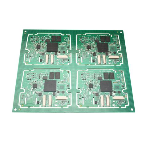
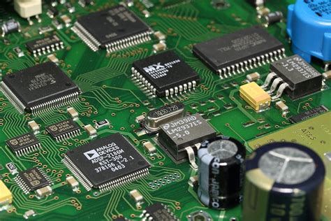
In terms of production, understanding various assembly techniques—commonly referred to as pcb assembly or PCBA—is vital for achieving reliability in electronic applications. Adaptations in these methodologies can lead to significant enhancements in performance while reducing costs. Furthermore, staying informed about advanced technologies such as surface mount technology (SMT) or through-hole technology can position designers to make informed decisions based on evolving industry standards.
The integration of robust testing methods during both design and production stages cannot be overstated. Implementing simulation tools allows for early detection of potential issues which could derail the functionality of the final product.
"Investing time in understanding the fundamentals of PCB design and fabrication can yield long-term benefits in terms of reliability and cost savings."
In conclusion, a thorough grasp of both design principles and fabrication methods empowers engineers to create effective solutions while optimizing resource usage throughout the lifecycle of the product.
Key Techniques for Optimizing PCB Design
Optimizing PCB design is crucial for achieving enhanced performance in various electronic applications. One of the fundamental techniques involves the careful layout of components to minimize signal integrity issues. For instance, maintaining short trace lengths and proper impedance matching can significantly reduce electromagnetic interference, thereby improving overall functionality. Additionally, utilizing advanced software tools for simulation during the design phase enables engineers to identify potential issues early and make necessary adjustments before going to PCB assembly. Selecting the right layers and carefully considering the placement of vias can further enhance thermal management and signal flow.
Another important aspect is the choice of materials during the fabrication process. Different substrates impact both performance and cost; high-frequency applications, for example, may require specialized materials like PTFE or Rogers laminate for optimal operation. Moreover, integrating components that facilitate easy PCBA can streamline assembly processes and reduce risks associated with manual assembly errors. Lastly, ongoing collaboration between design engineers and fabrication teams fosters a culture of continuous improvement, allowing new techniques to be implemented effectively throughout the stages of PCB development. By focusing on these techniques, organizations can not only enhance reliability but also ensure cost-effectiveness in their PCB endeavors.
Materials Selection: Impact on Performance and Cost
The choice of materials in PCB design plays a crucial role in determining both performance and cost efficiency. Different materials exhibit varying electrical, thermal, and mechanical properties, which can significantly impact the functionality of a Printed Circuit Board (PCB). For instance, using high-quality substrates such as FR-4 or Rogers can enhance the thermal management of electronic devices, resulting in improved signal integrity and overall performance. Conversely, opting for lower-cost materials might reduce production expenses but can compromise the reliability and efficacy of the finished product. Additionally, in the context of PCB assembly (PCBA), the selection of solder masks and finishes also affects adhesion, solderability, and corrosion resistance. Tailoring material choices according to specific application needs not only enhances performance but also minimizes total manufacturing costs throughout the lifecycle of the product. To maintain a competitive edge in an ever-evolving market, it is imperative to adopt strategic material selection that aligns with both functionality and budget constraints.
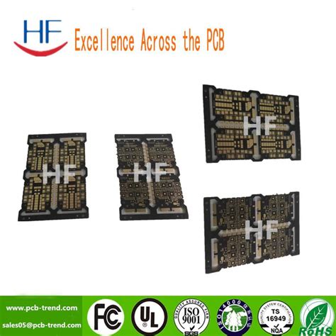
Advanced Fabrication Processes for Enhanced Reliability
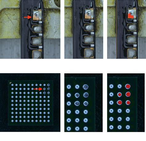
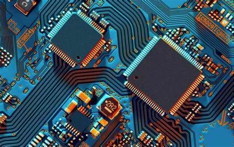
In the world of PCB design and fabrication, reliability is paramount, and advanced fabrication processes play a crucial role in achieving this goal. Techniques such as vacuum lamination and laser drilling offer significant advantages over traditional methods. Vacuum lamination ensures that layers are adhered uniformly, minimizing the risk of delamination, which can lead to circuit failures in electronic applications. Meanwhile, laser drilling provides precise hole placement and can create microvias that support high-density PCB assembly (often referred to as pcba). Furthermore, employing controlled impedance techniques during the fabrication process enhances signal integrity, ensuring that high-frequency signals travel with minimal loss. The implementation of these advanced processes not only bolsters reliability but also positions manufacturers to better meet the increasing demands for performance in modern electronics. Additionally, adopting robust quality control measures throughout fabrication can preemptively identify potential failures, thus reinforcing the durability of the final product. Overall, leveraging these sophisticated techniques enhances both functionality and longevity in pcba, making it an essential conversation in contemporary PCB design discussions.
Simulation and Testing: Ensuring Optimal Performance
In the realm of PCB design and fabrication, simulation and testing play a vital role in guaranteeing optimal performance. By utilizing advanced software tools during the design phase, engineers can predict how PCB assembly will function under various conditions. These simulations allow for the identification of potential issues, such as signal integrity problems or thermal management challenges, before physical prototypes are created. This proactive approach not only minimizes the risk of costly errors but also streamlines the overall fabrication process.
Moreover, it is essential to conduct rigorous testing on completed PCBA units to validate their performance against established specifications. Techniques such as thermal cycling, electrical performance testing, and environmental stress tests are crucial in assessing reliability and durability. By implementing a variety of simulation techniques alongside comprehensive testing protocols, manufacturers can enhance the overall quality of their products while reducing rework costs and improving time-to-market. Ultimately, these strategies contribute to creating robust electronics that better meet user demands and withstand the tests of time.
Cost-Effective Strategies in PCB Production
Optimizing PCB production processes involves several cost-effective strategies that can significantly enhance the overall performance of PCBs. The first step is to streamline the PCB assembly process by adopting modular designs that facilitate easier assembly, reducing both labor time and potential errors. Utilizing advanced pcba techniques like surface mount technology (SMT) not only increases component density but also enhances reliability. Moreover, selecting the right materials is crucial; opting for low-cost alternatives without compromising on quality can lead to significant savings. Additionally, exploring local fabrication services can minimize shipping costs and delivery times, thereby optimizing project timelines and budget allocation. Utilizing automation in the manufacturing process further contributes to cost reduction while maintaining high precision and consistency. By implementing these strategies, companies can produce more efficient and dependable PCBs, ensuring they meet the rigorous demands of today’s electronic applications while keeping costs under control.
Future Trends in PCB Design and Fabrication
As technology continues to evolve, the landscape of PCB design and fabrication is poised for significant transformation. One of the prominent trends is the increasing integration of AI-driven tools that aid in automating the PCB assembly process, enhancing both efficiency and accuracy. These tools not only streamline design workflows but also minimize human error, ensuring that the final product meets stringent quality standards. Additionally, there’s a growing shift towards using advanced materials, such as flexible substrates and conductive inks, which allow for greater innovation in product development. These materials not only improve performance but also facilitate miniaturization, opening new avenues for compact electronic devices.
Another noteworthy trend is the adoption of sustainability practices within the industry. Companies are increasingly prioritizing environmentally friendly materials and processes to reduce their carbon footprint. This encompasses everything from recyclable PCBs to processes that minimize waste during fabrication. Furthermore, there is an emphasis on open-source designs, which promote collaboration and sharing among engineers and designers across the globe.
Moreover, we anticipate a surge in demand for more sophisticated testing methods throughout the fabrication stages to ensure reliability in products designed for critical applications. This shift complements the trend toward increased functionality in PCBA (PCB assembly) processes that require high-density interconnections while maintaining thermal management capabilities.
Ultimately, these trends paint a promising picture for the future of PCB design and fabrication, combining advancements in technology with sustainability efforts to create more effective electronic solutions tailored to modern needs.
Case Studies: Success Stories of Optimized PCBs
In the realm of PCB design and fabrication, several notable case studies have showcased the substantial benefits of optimized processes. One prominent example involves a leading telecommunications company that sought to enhance the performance of its pcb assembly for a next-generation communication device. By employing advanced simulation tools, the engineering team was able to identify and rectify potential bottlenecks during the pcba phase, resulting in reduced signal interference and improved overall functionality. This optimization not only led to a more robust product but also cut production costs by 15%, illustrating that thoughtful design and fabrication strategies can yield significant financial and performance dividends.
Another influential case comes from the automotive industry, where a manufacturer integrated improved materials into their PCB solutions. By opting for high-frequency laminate materials, they achieved better thermal management, which is crucial for applications subjected to varying environmental conditions. This decision directly contributed to increased reliability and longevity of electronic systems in their vehicles, ultimately leading to lower warranty costs and enhanced customer satisfaction. These success stories exemplify how strategic enhancements in pcb design and its associated fabrication processes can lead to not just incremental improvements, but transformative results that pave the way for innovation across multiple sectors.
Conclusion
In summary, optimizing PCB design and fabrication is essential for achieving superior performance in electronic applications. The integration of advanced methodologies can lead to significant benefits, including enhanced reliability, decreased costs, and improved efficiency. For instance, careful materials selection plays a pivotal role; choosing materials that not only meet performance requirements but also minimize expenses can result in a notable impact on the overall PCB assembly process. Additionally, embracing state-of-the-art fabrication techniques ensures that the final product adheres to the highest quality standards. Techniques such as thorough testing and simulation before actual production further solidify the reliability of the final product, thereby enhancing the effectiveness of the entire design and manufacturing cycle. As industries continue to evolve, staying ahead through continuous innovation in pcba processes will be crucial for organizations aiming to maintain their competitive edge in this fast-paced market. Organizations that actively implement these optimization strategies are more likely to succeed in delivering high-quality electronic components that meet market demands efficiently.
FAQs
Q: What is PCB design and fabrication?
A: PCB design refers to creating a schematic layout of an electronic circuit that will be manufactured as a printed circuit board. Fabrication is the process of producing the physical board from that design, including layering, etching, and assembling components.
Q: Why is optimizing PCB design important?
A: Optimizing PCB design is crucial for enhancing performance, reducing manufacturing costs, and improving reliability. By fine-tuning the layout and component placement, designers can achieve better electrical performance and thermal management.
Q: What techniques can enhance PCB performance?
A: Techniques such as minimizing trace length, using ground planes effectively, selecting appropriate materials, and implementing simulation and testing can significantly enhance the performance of PCBs.
Q: How does material selection impact PCB fabrication?
A: The choice of materials affects both the performance and cost of a PCB assembly (PCBA). For example, high-frequency applications often require materials with specific electrical properties that might increase costs but are necessary for optimal functionality.
Q: What are some advanced fabrication processes?
A: Advanced processes include techniques like laser drilling, microvia technology, and fine line lithography. These methods improve reliability and allow for more complex designs.
Q: How can simulation contribute to PCB design optimization?
A: Simulation allows designers to analyze how a PCB will perform under various conditions without physical prototypes. This process helps identify potential issues early on, ensuring optimal performance in the final product.
For More Information on PCB Assembly
For those interested in learning more about effective strategies in pcb assembly, please click here.