Optimizing PCB Design & Manufacturing for Enhanced Technical Performance
Key Takeaways
Effective PCB design & manufacturing hinges on balancing technical precision with scalable production workflows. Prioritizing signal integrity and thermal management during the design phase reduces risks in pcb assembly, ensuring seamless transitions to PCBA (Printed Circuit Board Assembly). Key strategies include optimizing component placement for electromagnetic compatibility and leveraging design for manufacturability (DFM) principles to minimize errors.
Tip: Collaborate early with manufacturing partners to align design specifications with production capabilities, reducing costly iterations.
Incorporating automated optical inspection (AOI) and rigorous testing protocols enhances quality control in pcb manufacturing services, particularly for high-density interconnect (HDI) designs. Emphasizing material selection—such as low-loss laminates for high-frequency applications—directly impacts technical performance and long-term reliability. For cost-effective production, consider panelization techniques to maximize substrate utilization without compromising pcb performance metrics.
By integrating simulation tools like finite element analysis (FEA), teams can predict and mitigate mechanical stresses during pcb assembly, ensuring robustness in end-use environments. This alignment between design innovation and advanced manufacturing best practices drives efficiency and scalability across electronics projects.
PCB Design Optimization Strategies
Effective PCB design begins with strategic component placement to minimize signal interference and optimize thermal management. By leveraging advanced routing techniques—such as differential pair routing and controlled impedance traces—engineers can significantly enhance signal integrity in high-frequency applications. A critical step involves integrating Design for Manufacturing (DFM) principles early in the design phase to avoid costly revisions during PCB assembly.
For instance, optimizing pad sizes and spacing ensures compatibility with automated PCBA processes, reducing defects and rework. Additionally, employing thermal simulation tools helps identify hotspots, enabling proactive heat dissipation strategies like via stitching or copper pours.
| Design Factor | Traditional Approach | Optimized Strategy |
|---|---|---|
| Component Placement | Manual arrangement | Automated tools for density balance |
| Signal Integrity | Basic trace routing | Impedance-matched differential pairs |
| Thermal Management | Post-design fixes | Pre-layout simulation & modeling |
| DFM Compliance | Post-design adjustments | Early-stage rule integration |
Collaboration between design and PCB assembly teams ensures alignment on material selection, layer stack-up, and solder mask requirements. By prioritizing modular design principles, engineers can streamline prototyping and accelerate time-to-market for complex PCBA projects. These strategies not only improve technical performance but also lay the foundation for scalable, cost-efficient manufacturing.
Enhancing PCB Manufacturing Efficiency
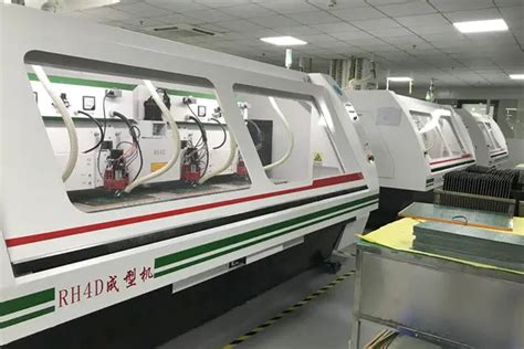
Achieving peak efficiency in PCB manufacturing requires a strategic blend of advanced processes and precision-driven workflows. By integrating automated PCB assembly systems, manufacturers can significantly reduce human error while accelerating production cycles. Modern surface-mount technology (SMT) enables high-speed placement of components during PCBA, ensuring tighter tolerances and improved repeatability. To further optimize efficiency, manufacturers are adopting design-for-manufacturability (DFM) principles early in the design phase, which minimizes rework by aligning layouts with production capabilities.
Lean manufacturing techniques, such as real-time monitoring of PCB assembly lines, help identify bottlenecks and reduce material waste. For instance, implementing predictive maintenance on pick-and-place machines ensures uninterrupted throughput, while advanced solder paste inspection (SPI) systems enhance first-pass yield rates. Additionally, leveraging PCBA-specific analytics tools allows for data-driven adjustments, such as optimizing thermal profiles for reflow ovens or calibrating stencil designs for solder deposition.
Collaboration between design and manufacturing teams remains critical. By standardizing component libraries and streamlining bill-of-materials (BOM) validation, companies can avoid delays caused by mismatched specifications. These practices not only improve manufacturing agility but also lay the groundwork for scalable, cost-effective production—a cornerstone of technical excellence in electronics manufacturing.
Key Considerations for Reliable PCB Production
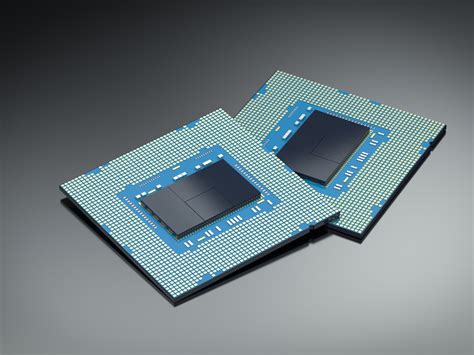
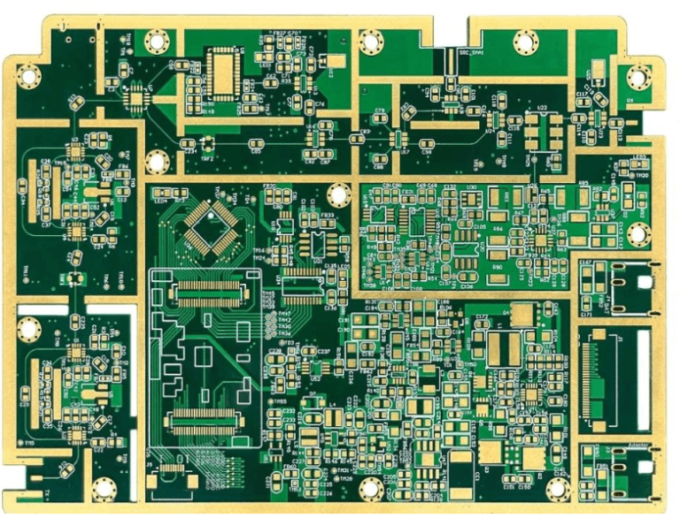
Achieving consistent reliability in PCB production demands meticulous attention to material selection, process control, and testing protocols. The choice of substrate materials, such as high-Tg FR-4 or polyimide, directly impacts thermal stability and signal integrity, particularly for high-frequency applications. During PCB assembly (PCBA), precise solder paste application and reflow profiling are critical to minimizing voids or cold joints, which can compromise long-term performance.
Automated optical inspection (AOI) systems play a pivotal role in detecting defects like misaligned components or insufficient solder coverage, ensuring adherence to IPC-A-610 standards. For complex designs, implementing design for manufacturability (DFM) guidelines reduces risks of fabrication errors, such as acid traps or uneven copper distribution. Additionally, environmental stressors—including humidity, thermal cycling, and vibration—must be simulated during reliability testing to validate PCBA durability under real-world conditions.
Collaboration between design and manufacturing teams is essential to balance performance requirements with production feasibility. By integrating advanced analytics into process monitoring, manufacturers can identify deviations in real time, enabling proactive adjustments. This holistic approach ensures that PCB assembly workflows deliver both technical precision and operational repeatability, forming the foundation for electronics that meet stringent reliability benchmarks.
Innovative Solutions in PCB Design Techniques
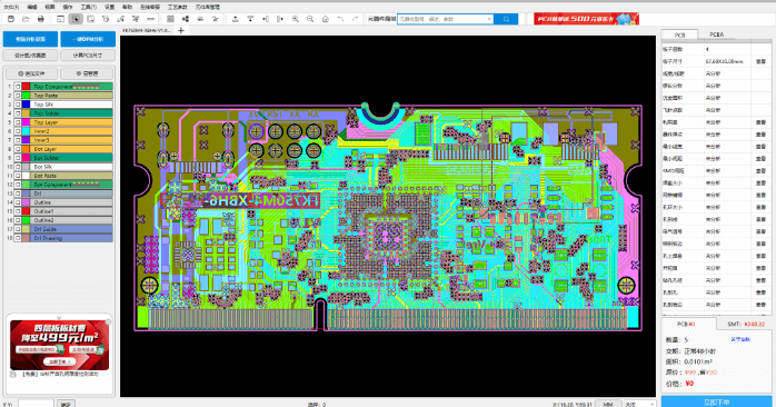
Modern PCB design leverages cutting-edge tools to address evolving technical demands. The integration of simulation-driven workflows enables engineers to predict thermal performance, signal integrity, and electromagnetic interference during early design stages. By employing automated routing algorithms, designers can optimize trace geometries while minimizing crosstalk and impedance mismatches, directly enhancing pcb assembly reliability. Another breakthrough lies in high-density interconnect (HDI) technology, which supports finer pitch components and multilayer stacking—critical for compact, high-performance devices.
Adoption of flexible PCB substrates further expands design possibilities, enabling conformal layouts for wearables and IoT applications. To streamline pcba processes, advanced design-for-manufacturing (DFM) principles are embedded into software platforms, flagging potential production issues like solder mask misalignment or insufficient pad spacing. Embedded passive components represent another innovation, reducing board footprint and improving signal speed by eliminating discrete parts.
Collaborative tools that synchronize schematic capture, layout, and pcb assembly testing data ensure seamless transitions from design to production. These solutions not only accelerate time-to-market but also align with sustainability goals through material efficiency and reduced prototyping cycles. By harmonizing pcba requirements with design ingenuity, engineers unlock new levels of technical precision across consumer electronics, automotive systems, and industrial automation.
Advanced PCB Manufacturing Best Practices
Implementing advanced PCB manufacturing best practices requires balancing precision engineering with process optimization. Central to this approach is adopting automated optical inspection (AOI) systems during PCB assembly, which reduces human error by detecting micro-defects in solder joints and component alignment. For PCBA (Printed Circuit Board Assembly) processes, leveraging laser-direct imaging (LDI) enhances trace accuracy, particularly for high-density interconnect (HDI) designs.
A critical focus lies in material selection, where low-loss dielectrics and high-temperature laminates improve signal integrity and thermal resilience. Manufacturers are increasingly integrating real-time monitoring tools to track parameters like reflow oven profiles, ensuring consistency across production batches. Additionally, adopting design for manufacturability (DFM) principles early in the workflow minimizes post-production revisions, aligning with the broader theme of merging design and manufacturing efficiency.
Transitioning to lead-free soldering and halogen-free substrates not only meets environmental regulations but also elevates product reliability. Advanced techniques such as sequential lamination for multilayer boards and controlled impedance testing further refine performance metrics. By standardizing these practices, manufacturers achieve tighter tolerances in PCB assembly, reduce time-to-market for PCBA projects, and strengthen compliance with industry benchmarks like IPC-6012. This systematic approach ensures technical excellence while supporting the article’s emphasis on innovation and reliability across electronics production.
Integrating Design & Manufacturing for PCB Success
Achieving seamless integration between PCB design and manufacturing processes is critical for delivering high-performance electronics. By aligning design-for-manufacturability (DFM) principles with production capabilities, engineers can minimize errors, reduce lead times, and enhance product reliability. For instance, optimizing pad sizes or trace widths during the design phase directly impacts PCB assembly efficiency, ensuring smoother solder paste application and component placement in the PCBA stage.
A holistic approach involves cross-functional collaboration, where design teams use simulation tools to predict thermal or signal integrity challenges, while manufacturing experts provide feedback on material compatibility and process limitations. This synergy reduces costly redesigns and accelerates time-to-market. Advanced PCB assembly workflows, such as automated optical inspection (AOI) paired with design data, further bridge gaps by validating layouts against real-world production parameters.
Moreover, adopting PCBA-centric prototyping enables iterative testing of both electrical and mechanical performance. Techniques like embedded component placement or rigid-flex designs demand tight coordination to balance innovation with manufacturability. By unifying these phases, organizations unlock scalable solutions that meet evolving technical demands while maintaining cost efficiency—a cornerstone of modern electronics development.
Cost-Effective PCB Production Methods
Balancing budgetary constraints with technical requirements remains central to optimizing PCB manufacturing workflows. A foundational strategy involves material rationalization – selecting substrate materials and copper weights that meet performance benchmarks without over-specification. Implementing design for excellence (DFX) principles during the PCB design phase minimizes costly revisions by aligning layouts with manufacturing capabilities, particularly for complex PCBA (printed circuit board assembly) configurations.
Automated PCB assembly lines enhance cost efficiency through precision component placement and reduced manual intervention, critical for high-volume orders. Standardizing surface finishes and solder mask options across product lines simplifies procurement and reduces material waste. Manufacturers can further leverage economies of scale by consolidating orders or utilizing panelization designs that maximize substrate utilization.
For low-volume prototypes, modular testing approaches focusing on critical functional areas reduce quality control expenses. Advanced PCB manufacturing partners often employ predictive analytics to optimize inventory management and machine uptime, ensuring lean production cycles. By integrating these methods, businesses achieve per-unit cost reductions of 15–30% while maintaining compliance with technical reliability standards essential for aerospace, medical, and industrial applications.
PCB Performance Metrics for Technical Excellence
To achieve technical excellence in PCB design & manufacturing, engineers must prioritize measurable performance metrics that align with functional and operational demands. Critical parameters like signal integrity, thermal management, and impedance control directly influence the reliability of PCBA (printed circuit board assembly) outcomes. For instance, maintaining consistent trace width and minimizing crosstalk ensures stable signal transmission, particularly in high-frequency applications. Thermal performance metrics, including heat dissipation rates and thermal resistance, are equally vital to prevent component degradation during PCB assembly processes.
Advanced testing protocols, such as automated optical inspection (AOI) and in-circuit testing (ICT), validate PCBA quality by identifying defects like solder bridging or misaligned components. Additionally, material selection—such as high-Tg laminates or low-loss substrates—directly impacts durability under extreme environmental conditions. By integrating real-time data analytics into manufacturing workflows, teams can optimize PCB assembly yields while adhering to tight tolerances.
Transitioning from design to production, aligning these metrics with manufacturing efficiency ensures that innovations in PCB design techniques translate into scalable, high-performance end products. This holistic approach bridges the gap between theoretical specifications and practical execution, driving technical excellence across the electronics lifecycle.
Conclusion
The convergence of PCB design and manufacturing services forms the cornerstone of delivering high-performance electronic systems. By aligning design intent with production realities, engineers can mitigate risks in pcb assembly while accelerating time-to-market. Emphasizing collaboration between design teams and PCBA specialists ensures that thermal management, signal integrity, and component placement are optimized for both functionality and manufacturability.
Adopting advanced tools like simulation software and automated testing protocols strengthens quality control, reducing defects in pcb assembly workflows. Furthermore, leveraging modular design principles and standardized PCBA processes enhances scalability across diverse projects. As industries demand faster, smaller, and more energy-efficient devices, integrating material innovation—such as high-frequency substrates or flexible circuits—into PCB design & manufacturing becomes critical.
Ultimately, success hinges on balancing technical precision with cost-efficiency. Continuous refinement of manufacturing best practices, paired with proactive adoption of emerging technologies, positions organizations to meet evolving performance benchmarks while maintaining robust production timelines. This holistic approach not only elevates product reliability but also drives sustainable innovation in electronics development.
FAQs
How does integrating design and manufacturing improve PCB performance?
Integrating PCB design and manufacturing processes ensures alignment between theoretical models and practical execution. Early collaboration minimizes design flaws, reduces rework cycles, and accelerates time-to-market. For instance, PCBA (Printed Circuit Board Assembly) teams can provide feedback on component placement to avoid soldering issues during production.
What distinguishes a standard PCB from a PCBA?
A PCB refers to the bare board with conductive pathways, while a PCBA includes assembled components soldered onto the board. The transition from PCB to PCBA involves precise PCB assembly processes, such as surface-mount technology (SMT) or through-hole mounting, to create functional electronic systems.
What are the key factors in ensuring reliable PCB production?
Reliability hinges on material selection, thermal management, and rigorous testing protocols. High-quality substrates, controlled impedance traces, and automated optical inspection (AOI) during PCB assembly help mitigate failures. Environmental stress testing further validates performance under extreme conditions.
How can manufacturers balance cost and quality in PCB assembly?
Adopting design for manufacturability (DFM) principles reduces material waste and assembly errors. Bulk purchasing of components and leveraging advanced PCBA techniques, like panelization, optimizes resource use. Partnering with certified PCB assembly providers ensures access to cost-effective yet high-precision solutions.
What innovations are shaping modern PCB design techniques?
Emerging trends include high-density interconnect (HDI) layouts, embedded components, and flexible PCB substrates. These advancements, combined with AI-driven PCBA analytics, enable tighter tolerances and enhanced signal integrity for cutting-edge applications.
Explore Professional PCB Assembly Solutions
For tailored PCB assembly services that prioritize technical excellence, please click here to connect with industry-leading expertise.