Optimizing PCB Manufacturing Workflows for Enhanced Efficiency
Key Takeaways
When optimizing workflows in PCB manufacturing, understanding core efficiency drivers helps balance speed with precision. First, automating assembly processes enables PCB manufacturing companies to reduce human error while accelerating output—critical for meeting tight prototyping deadlines. Implementing laser drilling and automated optical inspection (AOI) ensures micron-level accuracy, directly impacting PCB manufacturing cost by minimizing material waste.
A comparative approach reveals how optimized workflows outperform traditional methods:
| Metric | Traditional Workflow | Optimized Workflow |
|---|---|---|
| Prototyping Cycle | 14-21 days | 5-7 days |
| Defect Rate | 8-12% | <2% |
| Cost per Unit | $18.50 | $12.80 |
For PCB manufacturing business models, integrating digital twin simulations allows real-time design validation, slashing iteration time by 40%. Additionally, adopting just-in-time inventory practices reduces lead times while aligning with sustainable manufacturing goals—cutting excess material use by up to 30%. To maintain competitiveness, prioritize tools like AI-driven testing platforms that automate fault detection, ensuring error-free boards without manual intervention.
By focusing on scalable automation and data-driven decision-making, you can transform production bottlenecks into streamlined processes, ultimately enhancing both throughput and profit margins.
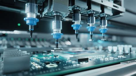
Automating PCB Assembly for Rapid Output
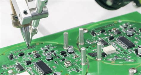
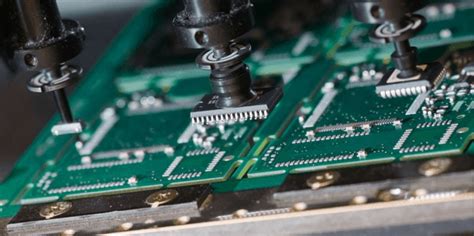
Implementing automation in PCB manufacturing transforms production floors from manual bottlenecks to high-speed precision hubs. By integrating robotic pick-and-place systems and AI-driven optical inspection tools, time-intensive tasks like component placement and solder paste application become error-resistant processes. For PCB manufacturing companies, this shift slashes assembly cycles by up to 60%, enabling same-day turnarounds for complex designs while maintaining consistent quality.
Advanced conveyor systems synchronize with surface-mount technology (SMT) lines, minimizing human intervention and reducing PCB manufacturing cost through material waste reduction. For instance, automated stencil printers ensure exact solder deposition, eliminating rework expenses. Real-time monitoring software further optimizes throughput by identifying workflow inefficiencies—critical for scaling a PCB manufacturing business without compromising on delivery timelines.
Transitioning to automation also future-proofs operations. Modular systems allow quick reconfiguration for varying batch sizes, making it easier to pivot between prototyping and mass production. This flexibility, paired with predictive maintenance algorithms, ensures machinery uptime remains above 95%, directly addressing client demands for rapid, reliable output in competitive markets. By prioritizing smart automation, you not only accelerate assembly but create a foundation for end-to-end digital integration across the entire production chain.
Precision Techniques in PCB Fabrication
Modern PCB manufacturing relies on advanced precision methods to ensure reliability while managing pcb manufacturing cost. High-density interconnect (HDI) technology, for instance, enables tighter trace spacing, critical for compact designs. Laser direct imaging (LDI) eliminates photomasks, reducing alignment errors and accelerating prototyping—a game-changer for pcb manufacturing companies aiming to balance speed with accuracy.
"Investing in automated optical inspection (AOI) systems can reduce defect rates by up to 70%, ensuring quality without inflating production timelines."
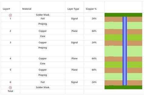
For multi-layer boards, controlled-depth drilling and sequential lamination ensure layer-to-layer alignment within ±25µm. These techniques minimize signal loss, especially in high-frequency applications. Additionally, pcb manufacturing business operations benefit from impedance-controlled routing, which maintains signal integrity in complex layouts.
Using direct metallization instead of chemical processes cuts waste and lowers environmental impact, aligning with sustainable practices. Pairing these methods with real-time data analytics lets you refine tolerances dynamically, avoiding over-engineering.
To optimize workflows, prioritize suppliers offering in-process testing—this catches flaws early, reducing rework costs. By integrating precision-driven strategies, you not only enhance product performance but also strengthen competitiveness in fast-paced markets.
Cost-Effective Prototyping Workflow Solutions
When refining your PCB manufacturing processes, balancing speed and PCB manufacturing cost requires strategic prototyping workflows. Start by adopting design-for-manufacturing (DFM) principles to minimize material waste and simplify assembly steps. Leveraging modular design frameworks allows you to test individual circuit blocks independently, reducing the need for full-board revisions. Many PCB manufacturing companies now offer rapid-turn prototyping services, enabling you to validate designs in 48–72 hours without premium pricing.
Integrate simulation-driven iteration early in the development cycle to identify potential signal integrity or thermal issues before physical production. Pairing this with automated design rule checks (DRCs) ensures compliance with your manufacturer’s capabilities, avoiding costly respins. For low-volume batches, consider hybrid workflows that combine subtractive and additive processes—this cuts material expenses by up to 30% while maintaining precision.
Collaborate closely with PCB manufacturing business partners to align prototyping timelines with bulk production schedules. Shared digital dashboards for real-time feedback on design adjustments streamline transitions from prototype to scaled manufacturing. By prioritizing cost-transparent workflows, you maintain budget control without sacrificing the iterative testing vital for complex PCB projects.
Smart Manufacturing for Reduced Lead Times
Adopting smart manufacturing strategies transforms how lead times are managed in PCB manufacturing. By integrating IoT-enabled sensors and machine learning algorithms, PCB manufacturing companies gain real-time visibility into production bottlenecks, enabling proactive adjustments. For instance, predictive maintenance systems analyze equipment performance data to schedule downtime before failures occur, minimizing unplanned delays. This approach not only accelerates throughput but also optimizes PCB manufacturing cost by reducing material waste and energy consumption.
Advanced analytics further refine process parameters, such as etching tolerances or solder paste application rates, ensuring first-pass yield improvements. Automated quality inspection systems, powered by AI vision, slash defect rates by over 40% compared to manual checks—critical for maintaining tight deadlines in high-volume orders. For PCB manufacturing business models prioritizing rapid turnaround, digital twin technology simulates design iterations virtually, cutting physical prototyping cycles by 30–50%.
Cloud-based collaboration platforms also synchronize workflows between design teams and fabrication units, eliminating communication lags. When paired with dynamic scheduling tools, these solutions compress PCB manufacturing timelines without compromising precision—a competitive edge in industries like aerospace or medical devices where speed-to-market dictates success.
Integrating Digital Tools in PCB Production
Adopting digital tools transforms how PCB manufacturing workflows operate, enabling PCB manufacturing companies to bridge design and production gaps. By leveraging advanced CAD/CAM software, you gain real-time visibility into design iterations, reducing manual adjustments and accelerating time-to-market. Cloud-based collaboration platforms allow engineers and fabricators to synchronize changes instantly, minimizing errors that inflate PCB manufacturing cost during prototyping.
IoT-enabled equipment further optimizes precision by collecting process data—from solder paste application to component placement—and feeding it into AI-driven analytics systems. This creates a feedback loop that refines tolerances and material usage, directly benefiting your PCB manufacturing business through reduced waste. For instance, predictive maintenance algorithms cut downtime by 30-40% in automated assembly lines, ensuring consistent output quality.
Transitioning to digital workflows also simplifies compliance tracking, as blockchain-based documentation automates traceability across suppliers. When paired with machine learning models that forecast demand fluctuations, these tools help balance inventory levels and production schedules. The result? A leaner operation where cost-efficiency and agility coexist—critical for staying competitive in high-mix, low-volume markets.
Optimizing PCB Testing for Error-Free Results
To ensure flawless performance in PCB manufacturing, rigorous testing protocols are non-negotiable. Modern PCB manufacturing companies leverage automated optical inspection (AOI) and X-ray inspection systems to detect microscopic defects like soldering flaws or trace misalignments. By integrating these tools early in production, you reduce PCB manufacturing cost by minimizing rework and material waste. Advanced electrical testing, such as flying probe or boundary-scan methods, validates circuit functionality at speeds up to 30% faster than manual checks, accelerating time-to-market.
For multi-layer designs, impedance testing becomes critical to maintain signal integrity, especially in high-frequency applications. Pairing these techniques with machine learning algorithms allows predictive error analysis, flagging potential failures before prototypes even reach assembly. This proactive approach strengthens your PCB manufacturing business by building reliability into every batch.
To optimize workflows further, synchronize testing data with design software. Real-time feedback loops help engineers adjust layouts iteratively, preventing recurring issues. Remember: investing in smart test jigs or modular fixtures enhances scalability, letting you adapt quickly to design changes without halting production. By prioritizing precision at this stage, you safeguard product quality while keeping lead times competitive.
Streamlining Multi-Layer PCB Design Processes
To optimize PCB manufacturing workflows, refining multi-layer design processes is critical. Modern design automation tools enable you to visualize layer stackups, route traces efficiently, and validate signal integrity early in the design phase. By adopting model-based systems engineering (MBSE), PCB manufacturing companies can reduce iterative revisions, cutting PCB manufacturing cost by up to 30% in prototyping stages.
Integrating collaboration platforms ensures seamless communication between design and fabrication teams, minimizing errors that delay production. For instance, using standardized design rule checks (DRCs) tailored to your PCB manufacturing business prevents mismatches in layer alignment or material specifications. Advanced tools like 3D thermal simulation further streamline workflows by predicting hotspots before physical prototyping, saving both time and resources.
Prioritizing modular design principles also accelerates scalability. By reusing validated circuit blocks across projects, you avoid redundant testing and speed up time-to-market—a key advantage in competitive markets. Pairing this with cloud-based version control ensures all stakeholders access the latest design iterations, reducing miscommunication risks.
Ultimately, these strategies not only enhance precision but create a foundation for sustainable growth, aligning multi-layer PCB design with broader goals of efficiency and cost-effectiveness in PCB manufacturing.
Sustainable Practices for Efficient PCB Manufacturing
Adopting eco-conscious strategies in PCB manufacturing isn’t just about environmental responsibility—it’s a competitive advantage. By prioritizing material efficiency, you reduce waste in copper etching and laminate usage, directly lowering PCB manufacturing cost while conserving resources. Leading PCB manufacturing companies now integrate renewable energy systems, such as solar-powered facilities, to minimize carbon footprints without compromising production speed.
Closed-loop recycling further enhances sustainability. For instance, reclaiming precious metals from discarded boards cuts raw material expenses and aligns with global e-waste regulations. Transitioning to lead-free soldering and halogen-free substrates not only meets compliance standards but also appeals to environmentally conscious clients, strengthening your PCB manufacturing business reputation.
Smart resource allocation plays a dual role: optimizing energy use with AI-driven machinery reduces operational costs, while modular designs simplify repairs and upgrades, extending product lifecycles. These practices ensure that sustainability and efficiency coexist, creating a workflow where lean principles and eco-innovation drive long-term profitability.
By embedding sustainability into every stage—from design to delivery—you future-proof operations against regulatory shifts and market demands, positioning your enterprise as a leader in both quality and responsibility.
Conclusion
Adopting optimized workflows in PCB manufacturing requires balancing technical precision with strategic resource allocation. For PCB manufacturing companies looking to maintain a competitive edge, reducing PCB manufacturing cost hinges on integrating smart automation and refining design-to-production handoffs. By leveraging data-driven insights, you can identify bottlenecks in your PCB manufacturing business, whether in material waste, testing inefficiencies, or delayed prototyping cycles.
Transitioning to digitally integrated systems not only accelerates throughput but also enhances repeatability—critical for scaling multi-layer or high-density designs. Prioritizing sustainable practices, such as energy-efficient machinery or recyclable substrates, further aligns operational efficiency with environmental responsibility. These steps collectively shorten lead times while maintaining the precision demanded by modern electronics.
Ultimately, success in PCB manufacturing depends on continuous improvement. Regularly auditing workflows, investing in staff training, and collaborating with suppliers ensure your PCB manufacturing business remains agile amid evolving industry standards. By focusing on holistic optimization, you transform cost challenges into opportunities for innovation and long-term growth.
Frequently Asked Questions
How does automation impact PCB manufacturing timelines?
Automation reduces manual intervention in PCB manufacturing companies, enabling faster assembly and testing. By integrating robotic systems, you can cut prototyping cycles by up to 40%, ensuring tighter deadlines are met without compromising quality.
What factors influence PCB manufacturing cost?
Material selection, layer complexity, and production volume are key drivers. PCB manufacturing businesses often optimize costs by balancing advanced materials with standardized processes, while digital tools like AI-driven design software minimize waste.
Can multi-layer PCB designs be streamlined for efficiency?
Yes. Using modular design principles and simulation software, you can simplify multi-layer layouts. Many PCB manufacturing providers offer pre-validated templates to accelerate development, reducing design iterations by 25–30%.
How do sustainable practices affect lead times?
Adopting eco-friendly materials or recycling programs may add initial planning time, but modern PCB manufacturing companies offset this by leveraging energy-efficient machinery, which maintains speed while lowering long-term operational costs.
What role do testing protocols play in reducing errors?
Automated optical inspection (AOI) and in-circuit testing (ICT) ensure precision in final products. By embedding these steps early in workflows, PCB manufacturing defects drop by over 50%, minimizing rework delays.
Ready to Optimize Your PCB Production?
For tailored strategies to reduce PCB manufacturing cost and scale your PCB manufacturing business, please click here to explore advanced solutions tailored to your needs.