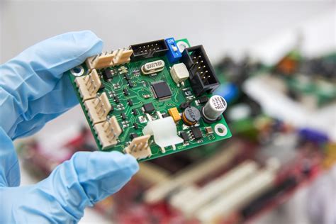
Optimizing Printed PCB Assembly for Reliable Manufacturing
Key Takeaways
Effective PCB assembly relies on three core pillars: precision design, strategic material selection, and rigorous quality control. Precision design forms the foundation, ensuring component placement accuracy and signal integrity through optimized trace routing and thermal management. This stage directly influences manufacturability, reducing errors in later PCBA phases. Material selection proves equally critical, with choices in substrate laminates, solder alloys, and conformal coatings determining long-term reliability under environmental stressors. Automated inspection systems like automated optical inspection (AOI) and X-ray testing provide multilayer defect detection, catching issues from solder bridging to component misalignment. When synchronized, these elements create a manufacturing workflow where efficiency gains in PCB assembly processes correlate with measurable quality improvements – typically demonstrated through reduced first-pass yield losses and improved mean time between failures (MTBF) in field operations.
Precision Design for PCB Assembly
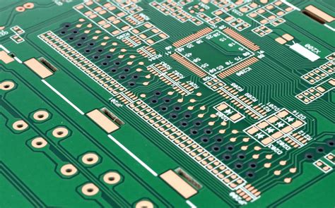
Effective PCB assembly begins with meticulous design strategies that balance functionality and manufacturability. Critical elements like component placement, trace routing, and layer stackup directly influence the reliability of PCBA (Printed Circuit Board Assembly). Modern design software enables engineers to simulate signal integrity and thermal performance, reducing errors before prototyping. For instance, optimizing pad sizes and solder mask clearances ensures compatibility with automated pick-and-place systems, minimizing defects during high-volume production.
Tip: Always align design specifications with PCB assembly capabilities. For example, maintain a minimum clearance of 0.2mm between components to avoid soldering issues.
A well-structured design also accounts for thermal management. Copper pours and strategically placed vias dissipate heat efficiently, preventing component failure. Below is a comparison of traditional vs. precision design approaches:
| Design Factor | Traditional Approach | Precision-Optimized Approach |
|---|---|---|
| Component Placement | Manual spacing adjustments | Algorithm-driven optimization |
| Trace Routing | Basic width rules | Impedance-controlled routing |
| Thermal Management | Passive heat sinks | Integrated thermal relief patterns |
| DFM (Design for Manufacturing) Checks | Post-design review | Real-time validation during design |
Incorporating Design for Manufacturing (DFM) principles early reduces rework costs and accelerates time-to-market. Key considerations include avoiding acute angles in traces and ensuring uniform copper distribution. As one industry expert notes:
“Precision in PCBA design isn’t just about functionality—it’s about creating a blueprint that harmonizes with assembly workflows.”
By prioritizing precision, manufacturers achieve higher yields and consistent performance, laying the foundation for reliable PCB assembly processes.
Material Selection in PCB Manufacturing
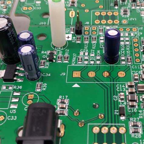
The foundation of reliable PCB assembly begins with strategic material selection, as substrate and component choices directly influence thermal performance, mechanical stability, and signal integrity. For PCBA applications, engineers prioritize laminates like FR-4 for its cost-effectiveness and balanced dielectric properties, while high-frequency designs may demand specialized materials such as Rogers substrates to minimize signal loss. Copper weight and thickness are equally critical, affecting current-carrying capacity and heat dissipation in high-power circuits.
Adhesives and solder masks must align with operational demands—lead-free solders and halogen-free laminates are increasingly adopted to meet environmental regulations without compromising joint reliability. For harsh environments, materials like polyimide flex substrates or metal-core boards enhance durability against thermal cycling and mechanical stress.
A systematic approach to material compatibility ensures seamless integration during PCB assembly, reducing risks of delamination or warping. Advanced PCBA workflows incorporate material databases with thermal expansion coefficients and moisture absorption rates to preempt manufacturing defects. By pairing rigorous material testing with real-world performance data, manufacturers achieve consistent results across production batches, bridging design intent with manufacturable outcomes.
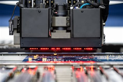
Automated Inspection Techniques Explained
Modern PCB assembly processes rely heavily on automated inspection techniques to ensure precision and minimize defects. Automated optical inspection (AOI) systems, for example, use high-resolution cameras and machine learning algorithms to scan PCBA boards for solder joint integrity, component misalignment, or missing parts. These systems analyze thousands of points in seconds, flagging deviations from design specifications with sub-micron accuracy. Complementing AOI, X-ray inspection delves deeper, revealing hidden flaws like voids in ball grid arrays (BGAs) or internal layer misregistrations—critical for multilayer boards.
Another cornerstone is in-circuit testing (ICT), which validates electrical performance by probing test points to verify connectivity, resistance, and capacitance. By integrating these methods into PCB assembly workflows, manufacturers achieve real-time defect detection, reducing rework costs and accelerating time-to-market. Advanced systems now incorporate artificial intelligence to predict failure patterns, further refining quality control.
Transitioning seamlessly from design and material choices, automated inspection bridges the gap between theoretical precision and practical reliability. As PCBA demands grow more complex, these techniques ensure consistent adherence to industry standards while supporting scalable production—key pillars for optimizing manufacturing outcomes.
Enhancing PCB Assembly Efficiency
Achieving optimal efficiency in PCB assembly requires strategic integration of design, process automation, and workflow standardization. A critical starting point is streamlining component placement through design-for-manufacturing (DFM) principles, which minimize redundant traces and align pad geometries with PCBA equipment capabilities. By reducing rework risks early in the design phase, manufacturers can accelerate turnaround times while maintaining precision.
Automated workflows, such as surface-mount technology (SMT) lines, play a pivotal role in scaling production. High-speed pick-and-place systems, coupled with vision-guided calibration, ensure rapid yet accurate placement of micro-components. Pairing these systems with inline inspection modules creates a closed-loop process where defects are flagged in real time, preventing bottlenecks downstream.
Material handling also impacts efficiency. Implementing just-in-time (JIT) inventory management for substrates, solder paste, and ICs reduces idle time between batches. Additionally, standardized solder profiles for reflow ovens and wave soldering machines minimize trial-and-error adjustments, enabling consistent PCB assembly across high-volume orders.
Finally, data-driven analytics tools can uncover hidden inefficiencies. Monitoring metrics like mean time between failures (MTBF) or component misalignment rates allows manufacturers to refine processes iteratively. By harmonizing these strategies, PCBA providers achieve faster cycle times without compromising the reliability demanded by modern electronics.
Consistent Production Quality Methods
Achieving uniformity in PCB assembly demands systematic approaches that address both process control and validation. Central to this is establishing standardized operating procedures (SOPs) for every stage, from solder paste stenciling to reflow profiling, which minimizes human error and ensures repeatable outcomes. Implementing statistical process control (SPC) enables real-time monitoring of critical parameters like component placement accuracy and solder joint quality, allowing immediate corrections before deviations escalate.
In PCBA production, combining automated optical inspection (AOI) with X-ray imaging provides multi-angle defect detection, catching issues ranging from tombstoning to insufficient solder fills. Post-assembly functional testing and boundary scan diagnostics further verify electrical performance against design specifications, creating layered quality assurance.
Material traceability systems ensure components meet specified tolerances, while environmental stress screening (ESS) exposes boards to thermal cycling and vibration, identifying latent failures. By correlating SPC data with PCBA test results, manufacturers gain actionable insights to refine processes iteratively. This closed-loop methodology not only sustains consistency but also drives continuous improvement, making it indispensable for high-reliability applications.
Optimizing PCB Manufacturing Processes
Effective PCB assembly optimization begins with streamlining design-to-production workflows. Implementing design for manufacturability (DFM) checks during prototyping reduces errors that could escalate costs in later stages. For PCBA processes, balancing speed with precision requires advanced equipment calibration, particularly in solder paste application and component placement. Integrating automated optical inspection (AOI) systems at critical stages ensures real-time defect detection, minimizing rework cycles.
Material flow management is equally vital. Adopting just-in-time inventory practices for components prevents delays while reducing storage costs. Pairing this with surface-mount technology (SMT) line optimizations, such as nozzle selection for pick-and-place machines, enhances throughput without compromising accuracy. Thermal profiling during reflow soldering also demands attention, as inconsistent heating can lead to latent failures in PCB assembly.
Finally, data-driven process control tools enable continuous improvement. Analyzing metrics like first-pass yield and mean time between failures helps identify bottlenecks. By aligning PCBA workflows with lean manufacturing principles, manufacturers achieve shorter lead times, higher reliability, and scalable production capacity—key factors in maintaining competitiveness.
Reliable PCB Assembly Best Practices
Achieving consistent reliability in PCB assembly requires adherence to rigorously tested methodologies. Central to this is implementing design-for-manufacturability (DFM) principles early in the development cycle, which minimizes risks of defects during PCBA production. For instance, maintaining proper pad-to-hole ratios and avoiding acute angles in trace routing reduces soldering inconsistencies. Pairing this with controlled material selection—such as high-Tg laminates for thermal stability—ensures boards withstand operational stresses.
Automated optical inspection (AOI) and X-ray inspection (AXI) systems further enhance reliability by identifying micro-cracks, voids, or misalignments invisible to manual checks. Integrating these tools with real-time data analytics allows manufacturers to refine processes like reflow profiling or stencil aperture designs. Additionally, standardized workflows for PCB assembly, including ESD-safe handling protocols and moisture-sensitive component storage, prevent environmental damage.
Collaboration between design and manufacturing teams is critical. Regular design reviews, coupled with prototype testing under simulated operating conditions, validate PCBA durability before mass production. By combining precision engineering, advanced inspection technologies, and cross-functional alignment, manufacturers can systematically eliminate failure points and deliver assemblies that meet stringent quality benchmarks.
Advanced Techniques for PCB Quality
Implementing cutting-edge methodologies ensures PCB assembly processes meet stringent quality benchmarks. Automated optical inspection (AOI) systems now leverage high-resolution cameras and machine learning algorithms to detect microscopic defects like soldering anomalies or misaligned components in PCBA units. For complex multilayer boards, X-ray inspection provides non-destructive analysis of hidden connections, ensuring internal integrity without compromising functionality. Advanced design for manufacturability (DFM) software further optimizes layouts by simulating thermal and mechanical stresses, preempting failures during prototyping.
Transitioning to in-circuit testing (ICT) enables real-time validation of electrical performance, identifying issues such as short circuits or open traces before mass production. Integrating predictive analytics into PCB assembly workflows also minimizes variability by correlating process parameters—like solder paste viscosity or reflow oven profiles—with historical quality data. This data-driven approach, combined with traceability systems, ensures rapid root-cause analysis for continuous improvement. By harmonizing these techniques, manufacturers achieve near-zero defect rates while maintaining alignment with evolving industry standards for PCBA reliability.
Conclusion
In the pursuit of reliable PCB assembly, integrating precision design with strategic material selection forms the cornerstone of manufacturing excellence. By prioritizing PCBA processes that emphasize thermal management and signal integrity, manufacturers can mitigate risks of failure while enhancing production throughput. The adoption of automated inspection techniques, such as automated optical inspection (AOI) and X-ray testing, ensures defects are identified early, maintaining consistency across batches. Furthermore, optimizing PCB assembly workflows through data-driven process controls and standardized protocols reduces variability, enabling scalable solutions for high-volume demands. As industries push toward miniaturization and higher complexity, aligning PCBA practices with evolving technological standards—such as Design for Manufacturability (DFM) principles—becomes critical. This holistic approach not only elevates product reliability but also strengthens competitive advantage in markets where quality and speed are non-negotiable. Ultimately, the synergy between advanced engineering methodologies and rigorous quality assurance defines the future of printed PCB assembly in achieving manufacturing resilience.
FAQs
How does precision design impact PCB assembly reliability?
Precision design ensures proper component placement and trace routing, minimizing signal interference and thermal issues. Using DFM (Design for Manufacturing) principles reduces errors during PCBA, leading to higher yield rates and long-term reliability.
What materials are critical for high-performance PCB assembly?
FR-4 substrates, high-purity copper layers, and halogen-free laminates are essential for thermal stability and signal integrity. Material choices directly affect PCB assembly outcomes, especially in high-frequency or high-temperature applications.
Why are automated inspection techniques vital in PCBA?
Automated optical (AOI) and X-ray (AXI) inspections detect solder defects, misalignments, and micro-cracks with micron-level accuracy. These systems ensure consistency, reducing human error and post-production failures by up to 40%.
How can manufacturers improve PCB assembly efficiency?
Adopting panelization for batch processing and integrating pick-and-place robotics streamlines workflows. Real-time monitoring of solder paste application and reflow profiles further optimizes PCBA throughput without compromising quality.
What methods ensure consistent PCB assembly quality?
Statistical process control (SPC) tracks critical parameters like solder volume and component placement accuracy. Pairing this with environmental stress screening (ESS) verifies reliability under operational conditions.
What are the best practices for reliable PCBA?
Regular calibration of assembly equipment, adherence to IPC-A-610 standards, and moisture-sensitive component handling protocols prevent defects. Implementing traceability systems also aids in root-cause analysis for continuous improvement.
How do advanced techniques address PCB quality challenges?
3D solder paste inspection (SPI) and AI-driven defect classification reduce false positives. These technologies, combined with thermal cycling tests, ensure PCB assembly durability in demanding applications.
Ready to Optimize Your PCB Assembly Process?
For tailored solutions in PCBA design, prototyping, and volume production, please click here to explore our expertise and advanced manufacturing capabilities.