Optimizing Prototype PCB Assembly for Rapid Development

Key Takeaways
Effective PCB assembly for prototyping requires balancing speed, precision, and adaptability. Three core principles define success in PCBA workflows: design-for-manufacturability (DFM), material compatibility, and modular testing. First, DFM ensures layouts minimize fabrication complexities, such as avoiding ultra-fine pitch components that demand specialized equipment. Equally important is selecting high-temp substrates or low-loss dielectrics that align with your application’s thermal and signal integrity needs while accelerating PCB assembly processes.
Tip: Validate component availability early to avoid delays—substitute hard-to-source parts with pin-compatible alternatives during prototyping.
Another critical factor is integrating advanced assembly techniques, such as automated optical inspection (AOI) and 3D solder paste monitoring, to catch defects before they cascade into costly rework. By prioritizing test points and boundary scan access in designs, engineers can streamline debugging and reduce iteration cycles by up to 40%. These strategies not only enhance PCBA reliability but also create a foundation for scaling prototypes to full production. Finally, aligning with suppliers offering rapid-turn PCB assembly services ensures design feedback loops stay tight, directly supporting faster time-to-market goals.

Streamlining PCB Prototype Assembly
Efficient PCB assembly processes are foundational to accelerating prototyping cycles. To streamline PCBA workflows, engineers must prioritize design-for-manufacturability (DFM) principles, ensuring layouts align with automated assembly capabilities. This includes optimizing component placement for pick-and-place machines and minimizing complex routing that could delay fabrication.
| Factor | Traditional Approach | Streamlined Approach |
|---|---|---|
| Design Validation | Post-assembly testing | Real-time simulation tools |
| Component Sourcing | Manual vendor coordination | Digitized inventory management |
| Assembly Accuracy | Visual inspection | Automated optical inspection (AOI) |
Leveraging advanced PCBA technologies, such as laser-direct imaging and high-speed surface-mount (SMT) lines, reduces turnaround times by up to 40%. Additionally, adopting modular design frameworks allows reusable blocks across prototypes, cutting redundant engineering efforts. Close collaboration between design and PCB assembly teams ensures early detection of thermal or signal integrity issues, preventing costly mid-process revisions.
Material selection also plays a critical role—using standardized substrates and pre-certified components avoids compatibility delays. For high-mix prototypes, flexible assembly lines with quick-change tooling further enhance adaptability. By integrating these strategies, teams achieve seamless transitions from design validation to functional testing, directly supporting faster iteration and market readiness.
PCB Design for Rapid Prototyping
Effective PCB assembly begins with design choices that prioritize speed and adaptability. By leveraging advanced design automation tools, engineers can create layouts optimized for PCBA workflows, reducing manual adjustments during fabrication. Critical considerations include component placement strategies that minimize signal interference while ensuring adequate spacing for automated pick-and-place machines. Routing techniques such as controlled impedance traces and via-in-pad designs enhance signal integrity while accommodating high-density interconnects common in modern prototypes.
To accelerate iterations, designers should integrate design-for-manufacturability (DFM) checks early, identifying potential conflicts in solder mask alignment or pad sizing that could delay PCB assembly. Modular design principles, like reusable circuit blocks, further streamline revisions without requiring full redesigns. Thermal management must also be addressed through copper pours and thermal relief patterns to prevent overheating during testing phases.
Finally, maintaining clear documentation—including layer stack-up details and bill of materials (BOM) annotations—ensures seamless handoffs between design and PCBA teams. This alignment reduces misinterpretation risks, enabling faster turnaround for prototype validation.
Material Selection for Efficient PCBs
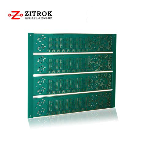
Strategic material selection forms the backbone of effective PCB assembly processes, directly influencing prototyping speed and functional reliability. Choosing the right substrate material, such as FR-4 for cost-effectiveness or polyimide for flexible applications, ensures compatibility with PCBA workflows while balancing thermal and mechanical demands. High-performance laminates with low dielectric loss minimize signal interference, critical for high-frequency prototypes.
For solderability and longevity, surface finishes like ENIG (Electroless Nickel Immersion Gold) or HASL (Hot Air Solder Leveling) must align with the PCB assembly environment. Conductive inks and adhesives should prioritize thermal conductivity to prevent overheating during testing phases. Additionally, selecting solder masks with rapid-cure properties reduces curing delays, accelerating PCBA timelines.
Material compatibility with automated pick-and-place systems is equally vital. Thin-core substrates and standardized thicknesses streamline component placement, while avoiding hygroscopic materials prevents warping during reflow soldering. By optimizing material choices for both electrical performance and manufacturability, engineers can significantly reduce prototype PCB assembly iteration cycles, paving the way for seamless transitions to volume production.

Advanced PCB Assembly Techniques
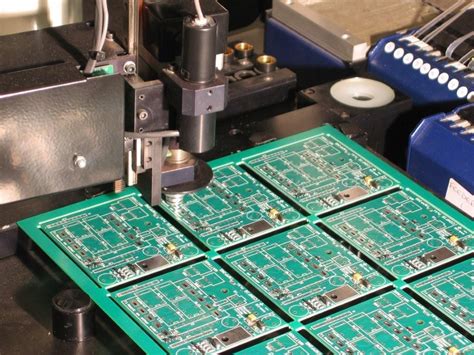
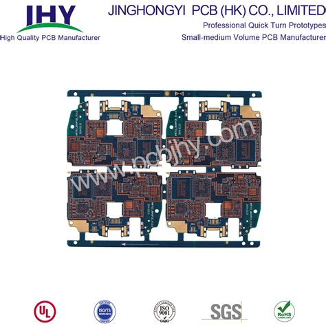
Modern PCB assembly processes leverage cutting-edge methodologies to address the complexities of rapid prototyping. Surface-mount technology (SMT) remains foundational, enabling high-density component placement with precision, while automated optical inspection (AOI) systems ensure error detection at micron-level accuracy. For PCBA workflows, integrating through-hole technology (THT) alongside SMT creates hybrid configurations that balance durability and miniaturization.
A critical advancement lies in design for manufacturability (DFM) principles, which optimize layouts for automated assembly, reducing manual rework. Engineers increasingly adopt sequential lamination for multilayer boards and laser-direct imaging to accelerate trace patterning. These techniques minimize alignment errors, a common bottleneck in prototype iterations.
Material innovation also plays a role: low-temperature co-fired ceramics (LTCC) and high-speed substrates enhance signal integrity in high-frequency applications. Additionally, 3D printing of solder masks allows rapid customization, aligning with dynamic design changes.
To further streamline PCB assembly, manufacturers now employ cloud-based collaboration tools for real-time design feedback, ensuring alignment between engineering and fabrication teams. By prioritizing modular test jigs and in-circuit testing (ICT) integration early in PCBA stages, teams can identify functional flaws before full-scale production.
These advancements collectively reduce turnaround times while maintaining reliability, making them indispensable for projects demanding both speed and precision.
Minimizing PCB Iteration Cycles
Reducing PCB assembly iteration cycles requires a systematic approach that integrates design validation, material compatibility, and collaborative PCBA processes. First-pass success begins with leveraging design verification tools to simulate thermal performance and signal integrity before physical prototyping. Implementing design for manufacturability (DFM) checks early ensures layouts align with PCBA capabilities, preventing rework due to pad spacing errors or incompatible component footprints.
Material selection plays a dual role: high-quality substrates like FR-4 or flexible polyimide minimize warping during soldering, while solder paste formulations optimized for reflow profiles reduce defects. Partnering with PCB assembly providers offering real-time feedback loops accelerates adjustments—for instance, swapping moisture-sensitive components or adjusting stencil apertures to address solder bridging.
Automated optical inspection (AOI) and in-circuit testing (ICT) further streamline validation by identifying assembly flaws before full-scale production. Adopting modular design principles allows isolated testing of critical subsystems, enabling targeted revisions without redesigning entire boards. By integrating these strategies, teams can compress iteration timelines by up to 40%, ensuring functional prototypes align with market-ready specifications.
Accelerating PCB Time-to-Market
Reducing PCB assembly timelines requires a holistic approach that bridges design, PCBA processes, and supply chain coordination. Time-to-market pressures demand rigorous alignment between design-for-manufacturability (DFM) principles and production workflows. By engaging PCB assembly partners early in the prototyping phase, engineers can preemptively address compatibility issues, such as component footprints or thermal management constraints, which often cause delays.
Leveraging just-in-time material procurement and standardized component libraries minimizes inventory bottlenecks, while automated PCBA processes—like surface-mount technology (SMT) and automated optical inspection (AOI)—ensure consistent quality without sacrificing speed. Additionally, adopting modular testing frameworks allows parallel validation of critical subsystems, slashing verification cycles by up to 40%.
To further compress timelines, prioritize design standardization across prototype iterations. Reusing validated circuit blocks and adhering to IPC-6012 guidelines for trace spacing reduces rework risks. Finally, integrating real-time collaboration tools between design teams and PCB assembly providers ensures rapid feedback loops, transforming weeks-long revisions into days. This synchronized strategy not only accelerates product launches but also builds a foundation for scalable manufacturing transitions.
Cost-Effective PCB Prototyping
Achieving cost-effective PCB prototyping requires balancing technical precision with budgetary constraints. While earlier sections addressed design optimization and PCB assembly techniques, financial efficiency demands strategic material selection and streamlined workflows. Start by evaluating low-volume production options that minimize waste without compromising quality—many PCBA providers offer tiered pricing models for prototype batches.
Leverage standardized component footprints to reduce custom tooling costs, and prioritize off-the-shelf parts over specialized ICs where feasible. Advanced PCB assembly services now integrate automated optical inspection (AOI) at the prototype stage, catching defects early and avoiding costly rework. For projects requiring rapid iteration, consider modular designs that allow partial updates instead of full-board revisions—a practice that slashes both time and material expenses.
Collaboration with suppliers is critical: negotiate bulk pricing for shared components across multiple prototypes and validate material specifications upfront to avoid mid-process substitutions. By aligning PCBA workflows with scalable design principles, engineers can maintain functional integrity while achieving up to 30% cost reduction in early-stage development. This approach not only preserves budgets but also ensures seamless transitions to mass production, reinforcing the financial viability of the entire product lifecycle.

Quality Control in PCB Prototyping
Effective PCB assembly processes rely on rigorous quality control measures to ensure prototypes meet functional and reliability standards. Critical inspection stages begin with verifying PCBA design files against manufacturing specifications, minimizing errors before physical production. Automated optical inspection (AOI) systems scan solder joints and component placements for defects, while X-ray imaging detects hidden flaws in high-density or multilayer boards.
Material integrity plays a pivotal role: thermal stress tests validate substrate durability, and cross-sectional analysis confirms plating quality in vias and traces. Statistical process control (SPC) tools monitor production variability, ensuring consistency across batches. For rapid development cycles, real-time feedback loops between assembly teams and designers help address issues early, reducing costly rework.
Advanced PCB assembly workflows integrate electrical testing protocols, such as in-circuit testing (ICT) or flying probe checks, to validate signal integrity and power distribution. Environmental stress screening (ESS) further simulates operating conditions to identify latent failures. By embedding quality checks at every stage, manufacturers accelerate time-to-market while maintaining compliance with industry standards like IPC-A-610. This systematic approach not only streamlines prototyping but also builds a foundation for scalable production.
Conclusion
Effective PCB assembly processes for prototypes require a holistic approach that aligns design, material selection, and manufacturing methodologies. By prioritizing PCBA techniques such as automated solder paste application and high-precision component placement, teams can significantly reduce errors and rework. Integrating design-for-manufacturability (DFM) principles early ensures compatibility with rapid prototyping workflows, while robust quality checks maintain reliability across iterations.
The interplay between PCB assembly speed and accuracy hinges on selecting advanced materials like high-Tg substrates or low-loss dielectrics, which support faster signal integrity validation. Additionally, leveraging modular testing frameworks during PCBA stages minimizes post-assembly debugging, directly contributing to shorter development cycles.
Ultimately, optimizing prototype PCB assembly is not just about accelerating timelines—it’s about creating a repeatable foundation for scaling production. By balancing agile methodologies with rigorous validation, teams achieve seamless transitions from prototype to mass manufacturing, ensuring market readiness without compromising performance or cost efficiency.
FAQs
How does design complexity impact prototype PCB assembly timelines?
Design complexity directly affects PCB assembly efficiency. Overly intricate layouts may require specialized component placement or multilayer routing, increasing fabrication time. Simplifying designs while maintaining functionality accelerates PCBA processes.
What material characteristics are critical for high-performance PCBA in prototypes?
Materials with high thermal stability and low signal loss are essential. Selecting substrates like FR-4 or polyimide ensures reliability during PCB assembly, while proper solder mask choices prevent short circuits in dense PCBA layouts.
How can DFM guidelines reduce iteration cycles during PCBA prototyping?
Adhering to Design for Manufacturability (DFM) principles minimizes rework. This includes optimizing pad sizes, ensuring adequate clearance, and avoiding non-standard components. Such practices streamline PCB assembly and reduce post-testing modifications.
What quality control measures ensure reliability in rapid PCB assembly?
Automated optical inspection (AOI) and X-ray testing are critical for detecting defects early. Combining these with functional testing validates PCBA performance, ensuring prototypes meet specifications before full-scale production.
Does opting for automated assembly affect time-to-market for prototypes?
Automated PCB assembly systems enable faster component placement and soldering, particularly for high-density designs. While initial setup may require time, the precision reduces errors, ultimately accelerating prototype validation and final product readiness.
Ready to Accelerate Your Prototype Development?
For tailored PCB assembly solutions that prioritize speed and precision, please click here to explore advanced PCBA services designed for rapid iteration and market-ready results.