Optimizing Signal Integrity in Assembled Circuit Board Design
Key Takeaways
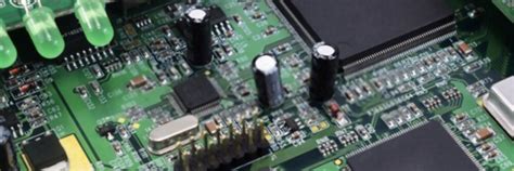
Effective PCB assembly requires careful consideration of signal integrity challenges, particularly in high-speed applications. Core principles include EMI reduction through proper shielding and component placement, optimized trace routing to minimize reflections, and strategic material selection to balance dielectric properties and cost. For PCBA designs, maintaining consistent impedance control and minimizing signal loss are critical for reliable data transmission.
| Technique | Key Impact | Application Consideration |
|---|---|---|
| EMI Shielding | Reduces electromagnetic interference | Critical for mixed-signal designs |
| Material Selection | Affects signal propagation speed | Match dielectric constant to frequency |
| Differential Pair Routing | Minimizes crosstalk and noise | Essential for high-speed interfaces |
Ground plane optimization plays a pivotal role in stabilizing reference voltages, while high-frequency PCB materials like Rogers substrates can enhance performance in RF applications. Designers must also address crosstalk prevention in dense layouts through adequate spacing and guard traces. By integrating these strategies during PCB assembly, engineers can achieve robust PCBA outcomes that meet both functional and reliability requirements.
EMI Reduction Strategies for PCB Signal Integrity
Effective EMI reduction begins with understanding interference sources in PCB assembly processes. Key approaches include implementing proper grounding schemes and minimizing loop areas through pcba-optimized component placement. Strategic use of ground planes reduces electromagnetic radiation by providing low-impedance return paths, while shielding techniques like metallic enclosures or conductive coatings contain high-frequency noise.
Tip: Always separate analog and digital ground regions during pcb assembly to prevent cross-coupling of noise-sensitive circuits.
For high-speed designs, differential pair routing and controlled impedance traces help cancel out common-mode interference. Decoupling capacitors placed near IC power pins in pcba designs suppress voltage fluctuations, further stabilizing signal integrity. Additionally, minimizing via transitions and avoiding sharp trace angles reduces unintended antenna effects.
Design Consideration: Use EMI filters on clock lines and I/O interfaces to attenuate high-frequency harmonics before they propagate.
Material choices also play a role—selecting substrates with lower dielectric losses (e.g., FR-4 with high Tg) minimizes signal degradation. By integrating these strategies early in the pcb assembly workflow, designers can achieve compliant EMI performance without compromising layout density or manufacturing feasibility.
High-Speed Trace Routing Best Practices
Effective high-speed trace routing is critical for maintaining signal integrity in PCB assembly designs, particularly as clock speeds and data rates increase. To minimize signal degradation and electromagnetic interference (EMI), designers must prioritize controlled impedance routing by matching trace widths to the dielectric properties of the substrate. For PCBA projects involving differential pairs, ensure symmetrical routing with consistent spacing to preserve signal balance and reduce common-mode noise.
Transitioning between layers introduces discontinuities, so limit the use of vias in high-speed paths. When unavoidable, employ back-drilling or blind vias to shorten stub lengths. Additionally, maintain a 3W rule (trace separation of three times the trace width) between parallel traces to mitigate crosstalk in dense layouts. For optimal performance, route high-speed signals over continuous ground planes to provide a low-impedance return path, avoiding splits or gaps that disrupt current flow.
Material selection also plays a role: high-frequency substrates like Rogers or Isola FR408HR, commonly used in advanced PCB assembly, offer lower dielectric losses for GHz-range applications. Finally, simulate designs using tools like HyperLynx to validate timing margins and impedance matching before finalizing the PCBA layout. These practices ensure reliable signal transmission while aligning with broader strategies for EMI reduction and thermal management.
Material Selection Impact on Circuit Performance
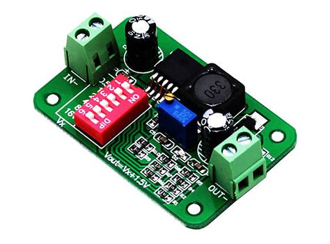
The choice of materials in PCB assembly directly influences signal integrity, thermal management, and long-term reliability. For high-frequency applications, substrates with low dielectric constant (Dk) and dissipation factor (Df), such as Rogers 4350B or Isola FR408HR, minimize signal attenuation and phase distortion. These properties are critical in PCBA designs where impedance matching and reduced crosstalk are priorities.
Copper weight and surface finish also play pivotal roles. Thinner copper layers (0.5 oz to 1 oz) reduce skin effect losses at high frequencies, while immersion silver or ENIG (Electroless Nickel Immersion Gold) finishes ensure consistent conductivity and corrosion resistance. For instance, in applications like the Reef-pi Deluxe Aquarium Controller, robust material selection ensures stable operation in humid environments.
Additionally, the dielectric material’s thermal stability affects performance under varying temperatures. Materials with high glass transition temperature (Tg), such as polyimide, maintain structural integrity during thermal cycling, preventing delamination in PCB assembly. Balancing cost and performance is essential—premium laminates may be justified for high-speed designs, while standard FR-4 suffices for less demanding applications. This strategic alignment of material properties with design requirements ensures optimal signal integrity across diverse PCBA use cases.

Ground Plane Optimization Techniques Explained
Effective ground plane design forms the backbone of reliable PCB assembly, particularly in high-speed and mixed-signal applications. A well-optimized ground plane minimizes electromagnetic interference (EMI), stabilizes reference voltages, and reduces impedance discontinuities that degrade signal integrity. For PCBA designs, engineers prioritize continuous copper pours over fragmented planes to ensure low-impedance return paths, which are critical for high-frequency signals.
Strategies such as split-plane isolation can mitigate noise coupling between analog and digital sections, while via stitching along the ground perimeter enhances current return efficiency. In multi-layer boards, dedicating entire layers to ground planes—paired with proper decoupling capacitor placement—helps suppress voltage fluctuations. However, designers must avoid excessive splits or slots in the ground plane, as these can create antenna effects that amplify EMI.
For PCB assembly workflows, material choice directly impacts ground plane performance. Low-loss substrates with consistent dielectric properties, such as FR-4 hybrids or specialized laminates, maintain impedance control across the plane. Additionally, aligning ground plane boundaries with critical signal layers in PCBA stacks ensures predictable return currents, reducing crosstalk in dense layouts. By balancing these techniques, engineers achieve robust signal integrity while accommodating the thermal and mechanical demands of modern electronics.
Minimizing Signal Loss in PCB Layouts
Effective PCB assembly processes rely on meticulous layout strategies to mitigate signal degradation, particularly in high-frequency applications. A critical factor is maintaining controlled impedance by optimizing trace geometry and ensuring consistent dielectric spacing. Impedance mismatches between components or traces can reflect signals, leading to attenuation, which is especially problematic in PCBA designs operating above 1 GHz. To address this, designers often prioritize shorter trace lengths, avoiding sharp angles (45° or curved bends preferred), and minimizing the use of vias—each of which introduces parasitic capacitance or inductance.
Material selection also plays a pivotal role, as substrates with lower dielectric loss tangents (e.g., Rogers or Isola laminates) reduce energy dissipation compared to standard FR-4. Additionally, proper ground plane implementation shields sensitive traces from electromagnetic interference (EMI), further preserving signal integrity. For multi-layer boards, symmetrical stack-ups help balance thermal and electrical stresses, preventing warping that could alter trace characteristics post-PCB assembly.
Finally, skin effect—where high-frequency currents migrate to a conductor’s surface—can exacerbate losses. Using wider traces or surface finishes like immersion silver mitigates this by increasing effective conductivity. By integrating these practices, engineers ensure reliable signal transmission in PCBA designs, laying the groundwork for subsequent discussions on crosstalk prevention in dense layouts.
Crosstalk Prevention in Dense PCB Designs
In dense PCB assembly layouts, crosstalk emerges as a critical challenge due to electromagnetic coupling between adjacent traces, particularly in high-speed PCBA applications. To mitigate this, designers must prioritize trace spacing and routing geometry. A practical approach involves maintaining a minimum spacing of 3x the trace width between parallel signal paths, reducing inductive coupling by up to 40%. For multi-layer designs, interleaving ground planes between signal layers creates shielding, effectively isolating sensitive traces.
Transitioning to differential pair routing further enhances noise immunity, as balanced signals inherently cancel out interference. When combined with controlled impedance routing, this technique ensures minimal signal degradation. Additionally, guard traces—grounded copper lines placed alongside high-speed traces—act as barriers to electromagnetic interference (EMI). For example, in a recent study, integrating guard traces reduced crosstalk by 28% in a 12-layer PCBA design.
Material selection also plays a pivotal role. High-frequency laminates with low dielectric loss (Dk < 3.5) minimize signal coupling, while avoiding sharp bends in traces prevents impedance discontinuities. Advanced simulation tools, such as 3D field solvers, enable pre-layout analysis of crosstalk risks, allowing iterative adjustments before finalizing the PCB assembly. By integrating these strategies, designers achieve robust signal integrity even in space-constrained, high-density environments.
High-Frequency PCB Material Selection
Selecting appropriate materials is critical for maintaining signal integrity in high-frequency PCB assembly designs. The dielectric constant (Dk) and dissipation factor (Df) of substrate materials directly influence signal propagation speed and loss, particularly in PCBA applications operating above 1 GHz. Low-loss laminates like Rogers RO4000® or PTFE-based substrates are preferred for their stable Dk values and reduced dielectric absorption, minimizing phase distortion in high-speed signals.
Thermal management also plays a pivotal role, as temperature fluctuations can alter material properties, leading to impedance mismatches. Materials with high glass transition temperatures (Tg) and low coefficient of thermal expansion (CTE) ensure dimensional stability during PCB assembly processes like reflow soldering. For instance, cleanliness requirements for assembled PCBs highlight the need for materials resistant to ionic contamination, which can degrade high-frequency performance.
Additionally, copper foil roughness must be optimized—smoother surfaces reduce skin effect losses at higher frequencies. By balancing electrical, thermal, and mechanical characteristics, designers can mitigate signal attenuation and crosstalk, aligning material choices with broader goals like EMI reduction and ground plane optimization. This strategic approach ensures reliable performance in demanding PCBA environments, from RF communications to advanced computing systems.
Differential Pair Routing Techniques
Effective differential pair routing is critical for maintaining signal integrity in high-speed PCB assembly designs. By ensuring precise trace spacing and length matching, designers can minimize electromagnetic interference (EMI) and crosstalk, which are common challenges in dense PCBA layouts. A well-executed differential pair configuration leverages balanced signals to cancel out noise, making it indispensable for applications like high-frequency data transmission or RF circuits.
To optimize performance, adhere to controlled impedance requirements by selecting materials with consistent dielectric properties, as highlighted in this analysis of high-quality circuit boards. Maintain symmetry between pairs by avoiding abrupt bends and using curved traces instead of right angles. Additionally, route differential traces over a continuous ground plane to reduce loop inductance and ensure consistent return paths. For multi-layer PCBA designs, prioritize adjacent layer pairing to minimize via-induced impedance discontinuities.
Advanced tools like length-tuning serpentines help compensate for mismatches caused by component placement or layer transitions. However, excessive meandering can introduce unwanted capacitance, so balance precision with practicality. Finally, validate designs through simulation to identify potential skew or phase imbalances before finalizing the PCB assembly process.
Conclusion
Achieving optimal signal integrity in PCB assembly requires a holistic approach that balances design precision with material science. While strategies like EMI reduction and ground plane optimization form the foundation, the choice of high-frequency PCB materials and meticulous differential pair routing directly influence performance in high-speed applications. For PCBA projects, prioritizing low-loss substrates and controlled impedance traces ensures minimal signal degradation, especially in densely packed layouts where crosstalk risks escalate.
Transitioning from design to production, collaboration with experienced PCB assembly partners becomes critical. Their expertise in implementing thermal management protocols and validating stack-up configurations can mitigate risks associated with high-frequency signal paths. Additionally, integrating advanced simulation tools during PCBA validation phases helps identify potential bottlenecks, such as reflections or impedance mismatches, before physical prototyping.
Finally, adherence to industry standards for conformal coating and environmental testing ensures long-term reliability. By harmonizing these elements, engineers can deliver assembled circuit boards that meet both functional and durability demands across diverse operating conditions.
FAQs
How does proper PCB assembly affect signal integrity?
During PCBA, component placement and soldering quality directly influence impedance matching and electromagnetic interference. Poorly aligned components or inconsistent solder joints can create signal reflections or crosstalk, degrading performance in high-speed designs.
What material properties are critical for high-frequency PCB assembly?
Materials with low dielectric loss (e.g., Rogers or FR-4 hybrid laminates) minimize signal attenuation at high frequencies. In PCBA, selecting substrates with stable thermal coefficients ensures consistent performance under varying operating conditions.
How can trace routing strategies reduce EMI in dense layouts?
Using differential pair routing and maintaining controlled impedance across traces helps cancel electromagnetic noise. For PCB assembly involving multilayer designs, shielding sensitive traces with grounded copper pours further isolates high-speed signals.
Why is ground plane optimization vital for signal integrity?
A continuous ground plane reduces loop inductance and provides a stable reference for signals. In PCBA, split or irregular ground planes can introduce ground bounce, especially in mixed-signal designs requiring precise voltage levels.
Can component placement impact crosstalk in PCB assembly?
Yes. Grouping high-speed components away from analog or power sections minimizes capacitive coupling. Additionally, orienting adjacent traces perpendicularly and increasing spacing between critical paths reduces unintended signal interference.
Ready to Optimize Your Next PCB Assembly Project?
For expert guidance on implementing these techniques in your PCBA designs, please click here to connect with our engineering team.