Optimizing Small Run PCB Assembly for Peak Performance
Key Takeaways
Effective PCB assembly for small production runs demands a balance between precision and cost-efficiency. By focusing on design optimization and streamlined workflows, manufacturers can reduce errors and accelerate timelines. Critical strategies include leveraging automated soldering for consistency and adopting design-for-manufacturing (DFM) principles to minimize rework.
"Investing in upfront design validation can prevent costly delays in PCBA projects, especially for prototypes or limited batches."
Key considerations for optimizing small run PCB assembly:
| Factor | Traditional Approach | Optimized Approach |
|---|---|---|
| Component Sourcing | Bulk orders | Just-in-time procurement |
| Testing | Post-assembly checks | In-line automated inspection |
| Turnaround Time | 2-3 weeks | 5-7 days (with modular tools) |
Prioritizing quality control through automated optical inspection (AOI) ensures defects are caught early, while panelization techniques maximize material usage. For cost-effective solutions, consider hybrid models combining manual oversight with automated pick-and-place systems.
Transitioning to the next section, these takeaways lay the groundwork for exploring precision techniques that further enhance reliability in PCB assembly workflows.
Enhancing Small Run PCB Assembly Efficiency
Achieving optimal efficiency in small run PCB assembly requires balancing speed, precision, and resource allocation. One foundational strategy is implementing design for manufacturability (DFM) principles early in the process, which minimizes rework by aligning layouts with PCBA capabilities. For instance, optimizing component placement reduces manual adjustments during soldering, directly improving throughput.
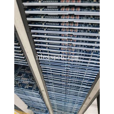
Material management is another critical factor. Procuring components with consistent lead times—and accounting for attrition rates—ensures uninterrupted workflows. Batch tracking systems further streamline inventory control, reducing delays caused by missing parts.
Leveraging modular tooling setups allows rapid reconfiguration between projects, a necessity for small run PCB assembly flexibility. Automated optical inspection (AOI) systems, when calibrated for low-volume batches, maintain first-pass yield without overburdening costs. Additionally, integrating just-in-time (JIT) workflows with contract manufacturers ensures synchronized timelines, preventing bottlenecks.
Finally, data-driven process audits identify inefficiencies like excessive solder paste application or misaligned pick-and-place operations. By refining these micro-steps, manufacturers can reduce cycle times by up to 20% while preserving PCBA reliability—a vital balance for electronics projects demanding both agility and precision.
Precision Techniques for Reliable PCB Production
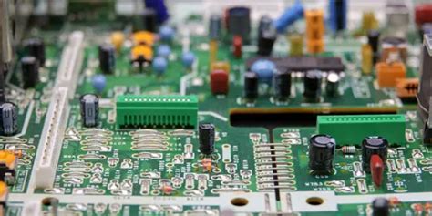
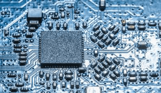
Achieving consistent reliability in PCB assembly requires meticulous attention to design specifications and manufacturing tolerances. For small run PCB assembly, precision begins with advanced surface-mount technology (SMT), which ensures components are placed with micrometer-level accuracy. Automated pick-and-place systems, paired with laser-aligned fiducial markers, minimize placement errors even in low-volume batches.
Critical to PCBA success is the integration of automated optical inspection (AOI) systems, which scan boards post-solder to detect defects like bridging or misalignment. For high-density designs, X-ray inspection further verifies hidden connections, such as those in ball grid arrays (BGAs). Thermal profiling during reflow soldering also plays a pivotal role, as precise temperature curves prevent stress fractures in delicate components.
Material selection further enhances reliability. Using high-Tg laminates and low-voiding solder paste improves thermal stability and electrical performance. Additionally, implementing design-for-manufacturing (DFM) checks early in the process reduces rework by addressing potential issues like pad spacing or solder mask misregistration.
This focus on precision not only elevates product quality but also aligns with cost-effective strategies by minimizing waste. As workflows transition to prototyping or scaling, these techniques ensure seamless compatibility with downstream processes like testing or enclosure integration.
Cost-Effective Strategies for PCB Assembly
Achieving cost efficiency in small run PCB assembly requires balancing precision with budget-conscious decisions. A critical first step is optimizing component sourcing—selecting suppliers offering volume-tiered pricing or consignment models for low-quantity orders. Leveraging standardized PCB assembly (PCBA) components, rather than custom parts, reduces material costs while maintaining functionality.
Implementing design for manufacturability (DFM) principles early minimizes rework risks. For instance, simplifying trace routing and avoiding overly complex layer stacks can lower fabrication expenses. Pairing this with automated pick-and-place systems ensures accurate component placement, even in small batches, reducing labor costs.
Another strategy involves hybrid manufacturing approaches. Combining automated surface-mount technology (SMT) for high-precision tasks with manual assembly for specialty components optimizes both speed and cost. Additionally, partnering with PCBA providers that offer shared panelization—grouping multiple designs onto a single production panel—can significantly cut per-unit costs.
Proactive testing protocols, such as in-circuit testing (ICT) or automated optical inspection (AOI), help catch defects early, avoiding costly post-production fixes. Finally, negotiating flexible payment terms or bundled services with PCB assembly partners ensures scalability without compromising quality. By integrating these strategies, manufacturers can maintain competitive margins while delivering reliable, high-performance electronics.
Quality Control in Small Batch PCB Manufacturing
Implementing rigorous PCB assembly quality protocols becomes critical when working with limited production volumes, where each unit’s performance directly impacts project outcomes. Advanced inspection tools like automated optical inspection (AOI) and X-ray imaging enable precise detection of soldering defects, component misalignment, or micro-cracks in PCBA units. For high-reliability applications, functional testing under simulated operational conditions validates electrical performance, while environmental stress screening (ESS) exposes boards to thermal cycling and vibration to identify early-life failures. Statistical process control (SPC) methods analyze production data to refine tolerances and minimize variability, ensuring consistency across batches. Additionally, traceability systems document material sources and assembly parameters, simplifying root-cause analysis if revisions are needed. By integrating these layered checks, manufacturers maintain exceptional standards even in low-volume PCB assembly, reducing rework costs and accelerating time-to-market for specialized electronics.
Optimizing PCB Design for Assembly Success
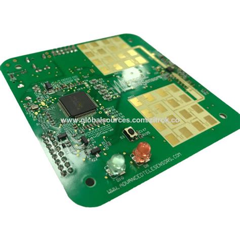
Effective PCB assembly begins with design choices that align with manufacturing realities. When preparing for small run PCBA, engineers must prioritize design for manufacturability (DFM) principles to minimize errors and rework. Key considerations include optimizing component placement for automated pick-and-place systems, ensuring adequate pad spacing for solderability, and selecting surface finishes compatible with PCB assembly workflows. For instance, incorporating fiducial markers and standardized panelization layouts can significantly improve alignment accuracy during PCBA, especially in low-volume batches.
Collaborating early with experienced manufacturers helps identify potential pitfalls, such as mismatched footprints or thermal imbalances, before prototyping. Advanced tools like 3D modeling software enable designers to simulate assembly compatibility, reducing risks of mechanical interference or soldering defects. Additionally, adhering to IPC-7351 standards for land patterns ensures seamless integration of components across PCB assembly stages. This proactive approach not only accelerates time-to-market but also enhances reliability in high-mix, low-volume production environments. By embedding DFM checks into the design phase, teams create a foundation for scalable, cost-efficient PCBA workflows—a critical advantage when transitioning from prototypes to full-scale manufacturing.
Streamlining Prototype PCB Assembly Workflows
Efficient PCB assembly workflows for prototypes require a balance between speed, accuracy, and adaptability. Unlike high-volume production, small-run PCBA projects demand agile processes that accommodate iterative design changes without compromising quality. Start by implementing design for manufacturability (DFM) checks early in the prototyping phase to identify potential bottlenecks, such as component spacing issues or incompatible footprints. Leveraging modular tooling and standardized panel layouts can reduce setup times while maintaining flexibility for design adjustments.
Integrating automated optical inspection (AOI) systems ensures consistent quality across prototypes, even with frequent revisions. For low-volume builds, hybrid workflows combining manual assembly for unique components and automated pick-and-place machines for standardized parts optimize both precision and cost-efficiency. Additionally, adopting digital twin simulations allows engineers to validate assembly sequences virtually, minimizing physical rework.
Collaboration between design and manufacturing teams is critical. Real-time communication via cloud-based PCBA platforms accelerates feedback loops, enabling rapid resolution of issues like solder mask misalignment or thermal management challenges. By refining these workflows, manufacturers can shorten lead times for prototype PCB assembly while ensuring seamless scalability to full production.
Automation Solutions for Small Run PCB Projects
Integrating automation into small-run PCB assembly processes bridges the gap between prototyping and mass production, enabling manufacturers to maintain precision while scaling operations. Advanced pick-and-place systems, optimized for low-volume batches, reduce manual handling errors and accelerate placement accuracy for intricate components. These systems, paired with AI-driven optical inspection (AOI) tools, ensure consistent quality by detecting soldering defects or misalignments early in the PCBA workflow.
For projects requiring flexibility, modular automation platforms allow rapid reconfiguration between different PCB assembly designs, minimizing downtime. Robotic soldering arms, for instance, adapt to varying component sizes and layouts, ensuring repeatability even in high-mix, low-volume environments. Additionally, automated inventory management systems track component usage in real time, preventing shortages and streamlining material sourcing for small-run PCBA orders.
However, balancing automation costs remains critical. Hybrid approaches—combining automated stages with selective manual oversight—optimize resource allocation without compromising efficiency. By leveraging cloud-based process monitoring, teams gain actionable insights to refine workflows, ensuring PCB assembly cycles align with project timelines. This strategic integration of automation not only enhances throughput but also positions small-run manufacturers to compete in markets demanding both agility and reliability.
Troubleshooting Common PCB Assembly Challenges
Identifying and resolving issues in PCB assembly requires systematic analysis of recurring problems. Solder bridging, component misalignment, and thermal stress rank among the most frequent challenges in PCBA workflows, particularly in small-run projects where process tolerances are critical. For instance, inadequate solder paste stencil alignment can lead to uneven deposition, causing opens or shorts during reflow. Implementing automated optical inspection (AOI) systems helps detect these defects early, while X-ray inspection proves invaluable for verifying hidden connections in multi-layer boards.
Another common pitfall involves component tombstoning, often triggered by uneven heating or mismatched pad sizes. Adjusting reflow profiles and ensuring symmetrical pad designs mitigate this risk. For electrical failures, such as intermittent connectivity, thorough testing with flying probe or boundary scan tools isolates faulty traces or soldered joints. Partnering with specialized providers like Entech’s OEM solutions ensures access to advanced diagnostic tools tailored for low-volume production.
Proactive troubleshooting also hinges on design-for-manufacturing (DFM) reviews to flag potential assembly conflicts, such as inadequate clearance for pick-and-place machines. By integrating real-time feedback loops between design and production teams, manufacturers can preemptively address challenges unique to small-run PCB assembly, optimizing both yield and reliability.
Conclusion
Achieving peak performance in small run PCB assembly requires a strategic balance between precision, cost-efficiency, and rigorous quality assurance. By integrating advanced PCBA techniques such as automated optical inspection (AOI) and laser-depaneling, manufacturers can minimize errors while maintaining scalability for low-volume projects. Prioritizing design-for-manufacturability (DFM) principles early in the process ensures smoother transitions from prototyping to production, reducing rework and material waste.
For cost-sensitive projects, leveraging modular tooling and partnering with specialized suppliers can optimize resource allocation without compromising on PCB assembly reliability. Additionally, implementing statistical process control (SPC) methods strengthens consistency across batches, even in small run environments.
As the demand for agile electronics manufacturing grows, staying updated with emerging trends like flexible PCBA workflows and IoT-enabled monitoring systems will further refine production outcomes. Ultimately, success hinges on aligning technical rigor with adaptable processes to meet evolving industry standards.
FAQs
Q: What defines a small run in PCB assembly, and how does it differ from mass production?
A: A small run PCB assembly typically refers to batches of 50 to 1,000 units, prioritizing flexibility and rapid iteration. Unlike mass production, it emphasizes cost-effective tooling adjustments and tailored PCBA workflows to accommodate design refinements.
Q: How can design optimizations improve assembly efficiency for low-volume projects?
A: Adopting design for assembly (DFA) principles—such as standardizing component sizes and minimizing complex layouts—reduces manual labor during PCB assembly. This accelerates prototyping and lowers error rates in small run PCBA processes.
Q: What quality control measures are critical for small batch manufacturing?
A: Automated optical inspection (AOI) and functional testing ensure consistency in PCB assembly. For small run PCBA, statistical process control (SPC) tracks defects early, while batch-level traceability simplifies troubleshooting.
Q: Can automation benefit low-volume PCB assembly, or is it only viable for large-scale production?
A: Modular automation tools, like pick-and-place systems with quick-change setups, enhance precision in small run PCBA without requiring high upfront investments. This balances speed and affordability for prototype-to-production transitions.
Q: How do material choices impact the reliability of small batch assemblies?
A: High-quality substrates and finishes (e.g., ENIG or HASL) prevent solder joint failures in PCB assembly. For PCBA projects, thermal management materials like polyimide flex circuits improve durability in compact designs.
Ready to Elevate Your Small Run PCB Assembly Workflow?
For tailored solutions that blend precision, cost-efficiency, and scalability, please click here to explore advanced PCB assembly services designed for low-volume innovation.