Optimizing SMD PCB Production: Manufacturer Selection Insights

Key Takeaways
When evaluating SMD PCB manufacturers, three core considerations dominate decision-making: technical competency, quality assurance protocols, and cost-efficiency. Manufacturers specializing in PCB assembly (PCBA) must demonstrate proficiency in handling high-density interconnect (HDI) designs, surface-mount technology (SMT), and mixed-technology boards. A robust quality management system, validated by certifications like ISO 9001 and IPC-A-610, ensures adherence to industry standards for reliability and durability.
"Selecting a manufacturer without auditing their process controls is like buying a car without test-driving it—always verify their defect rates and testing methodologies."
Below is a comparative analysis of critical factors for PCBA partnerships:
| Factor | High-Quality Focus | Cost-Driven Focus |
|---|---|---|
| Testing Protocols | Automated optical + X-ray | Basic functional testing |
| Material Sourcing | Tier-1 substrates/components | Value-engineered alternatives |
| Lead Time Flexibility | Agile, with expedited options | Standardized production runs |
Prioritize suppliers offering design for manufacturability (DFM) feedback, as this reduces time-to-market and minimizes redesign costs. While balancing cost and quality, avoid compromising on thermal management capabilities or solder joint integrity—critical for mission-critical applications. Advanced manufacturers now integrate AI-driven process optimization, enhancing yield rates in PCB assembly by up to 15%.
Selecting Top SMD PCB Manufacturers
Choosing the right SMD PCB manufacturer requires a balanced evaluation of technical expertise, production scalability, and compliance with industry standards. Start by assessing the manufacturer’s capabilities in PCB assembly processes, particularly their proficiency in handling high-density interconnect (HDI) designs and fine-pitch components. Advanced surface-mount technology (SMT) integration, such as automated pick-and-place systems and reflow soldering accuracy, directly impacts the reliability of PCBA outcomes.
Prioritize vendors with ISO-certified quality management systems and adherence to IPC-A-610/620 standards, ensuring consistent performance in PCB assembly workflows. Review their track record in delivering lead-free soldering solutions and mitigating risks like tombstoning or solder bridging—common challenges in SMD PCB production. Additionally, evaluate their material sourcing practices; partnerships with reputable substrate suppliers (e.g., FR-4, polyimide) enhance durability and thermal stability in finished assemblies.
Cost considerations should extend beyond per-unit pricing. Analyze their design-for-manufacturability (DFM) support, which reduces prototyping iterations and minimizes waste. Transparent communication about lead times, testing protocols (e.g., automated optical inspection (AOI)), and post-production services like conformal coating further streamline the PCBA lifecycle. By aligning these factors with your project’s technical demands, you ensure a partnership that optimizes both quality and efficiency in SMD PCB manufacturing.
Optimizing SMD Assembly Production
Achieving precision in PCB assembly requires manufacturers to balance advanced equipment with process refinement. Modern PCBA workflows demand high-speed pick-and-place machines capable of handling miniature Surface-Mount Devices (SMDs) while maintaining micron-level accuracy. Optimized production begins with rigorous Design for Manufacturability (DFM) checks, ensuring component layouts align with solder paste application and reflow profiles.
Critical factors include automated optical inspection (AOI) systems to detect solder bridging or misaligned components, paired with X-ray inspection for hidden defects in ball grid arrays (BGAs). Progressive manufacturers integrate real-time process monitoring to adjust parameters like temperature and conveyor speed, minimizing rework rates.
Material selection also plays a pivotal role—low-voiding solder pastes and moisture-resistant substrates enhance reliability in demanding environments. For cost-effective scaling, prioritize facilities offering flexible batch sizing without compromising turnkey PCB assembly timelines. By aligning technical capabilities with lean manufacturing principles, suppliers can reduce waste while ensuring consistent PCBA quality—a foundation for high-yield SMD production across consumer electronics, automotive, and IoT applications.
Quality Assurance in PCB Manufacturing
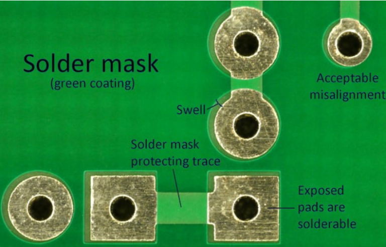
Robust quality assurance (QA) protocols form the backbone of reliable SMD PCB production, ensuring consistent performance across PCB assembly processes. Leading manufacturers implement multi-stage inspection systems, combining automated optical inspection (AOI) and X-ray testing to detect solder joint defects, component misalignment, and micro-cracks in high-density interconnects. These checks are critical for PCBA reliability, particularly in applications demanding precision, such as medical devices or aerospace electronics.
Certification compliance further validates QA effectiveness—look for ISO 9001, IPC-A-610, and IATF 16949 adherence, which demonstrate rigorous process control and defect prevention capabilities. Advanced producers also employ statistical process control (SPC) to monitor production variables in real time, minimizing deviations before they escalate. Material traceability, from substrate sourcing to final PCB assembly, ensures accountability across the supply chain, while environmental stress screening (ESS) simulates operational conditions to verify long-term durability.
By prioritizing these QA measures, manufacturers reduce field failure rates and align with evolving industry standards, ultimately delivering PCBA solutions that meet both technical specifications and end-user expectations.
Cost-Effective SMD Solutions Guide
Achieving cost efficiency in SMD PCB manufacturing requires balancing material optimization, process automation, and supplier partnerships. High-volume production often benefits from economies of scale, but selecting the right PCB assembly partner is critical to avoid compromising quality. Manufacturers leveraging advanced PCBA techniques, such as automated pick-and-place systems and reflow soldering, can reduce labor costs while maintaining precision. Prioritizing standardized component libraries over custom parts minimizes procurement delays and expenses.
Material selection plays a pivotal role—opting for cost-effective yet reliable substrates like FR-4 or low-loss laminates ensures performance without overspending. Additionally, implementing Design for Manufacturability (DFM) checks early in the design phase prevents costly revisions. For budget-conscious projects, consider suppliers offering volume-based pricing models or panelized production to reduce per-unit costs.
Testing strategies also impact affordability. Combining automated optical inspection (AOI) with targeted in-circuit testing (ICT) streamlines defect detection, avoiding full-scale testing expenses. Finally, partnering with PCB assembly providers that offer transparent pricing tiers and value-added services—such as component sourcing support—ensures alignment with both technical requirements and budgetary constraints.
Advanced SMD Technology Integration
Modern PCB assembly processes demand seamless integration of advanced surface-mount device (SMD) technologies to meet evolving industry standards. Leading manufacturers now deploy PCBA systems incorporating automated optical inspection (AOI) and 3D solder paste inspection (SPI), which enhance precision while minimizing defects. These systems optimize placement accuracy for ultra-fine-pitch components, such as 01005 resistors or micro-BGAs, ensuring compatibility with high-density interconnect (HDI) designs.
A critical advancement lies in the adoption of laser-direct imaging (LDI) for solder mask application, which eliminates phototool-related errors and supports tighter tolerances below 25µm. Pairing this with nitrogen-reflow soldering reduces oxidation risks, particularly for PCB assembly involving lead-free alloys like SAC305. For mission-critical applications, manufacturers leveraging embedded component technology achieve up to 30% space savings by integrating passive components within multilayer substrates—a strategy increasingly vital for IoT and wearable devices.
Moreover, smart factories employ machine learning-driven predictive maintenance to preempt equipment calibration drifts, maintaining ±0.025mm placement repeatability. This technological synergy not only accelerates PCBA throughput but also strengthens thermal management through advanced via-in-pad and copper-filled microvia designs. As surface-mount components shrink below 0.3mm², such innovations ensure manufacturers balance miniaturization demands with signal integrity preservation—a non-negotiable requirement for 5G and automotive electronics. By prioritizing these integrations, producers future-proof their capabilities while adhering to IPC-A-610 Class 3 standards for high-reliability assemblies.
Key Factors for Reliable PCB Assemblies
Achieving reliability in PCB assembly hinges on balancing technical precision with robust quality control frameworks. Material selection forms the foundation, where high-grade substrates, copper layers, and solder masks directly impact durability and thermal performance. Manufacturers must adhere to IPC-A-610 standards for solder joint integrity, particularly in PCBA involving surface-mount devices (SMDs), where micron-level alignment errors can compromise functionality.
Process optimization plays an equally critical role. Automated optical inspection (AOI) systems and X-ray imaging ensure defect detection in multilayer boards, while controlled reflow soldering profiles prevent issues like tombstoning or cold joints. For mission-critical applications, environmental stress testing—including thermal cycling and vibration simulations—validates assembly resilience under extreme conditions.
Supply chain transparency further strengthens reliability. Partnering with manufacturers that implement traceability systems for components mitigates risks of counterfeit parts, a growing concern in complex PCB assembly projects. Additionally, adherence to ISO 9001-certified workflows ensures consistent process documentation, reducing variability across production batches.
Finally, design-for-manufacturability (DFM) collaboration between engineers and producers identifies potential failure points early, optimizing layouts for efficient PCBA processes without sacrificing performance. This proactive approach, combined with rigorous post-assembly testing, establishes a holistic framework for delivering dependable electronic assemblies.
Evaluating Cutting-Edge PCB Producers
When assessing PCB assembly providers, technical capability remains a critical differentiator. Leading SMD PCB manufacturers distinguish themselves through investments in automated optical inspection (AOI) systems, high-precision pick-and-place machinery, and laser direct imaging (LDI) technologies. These advancements ensure tighter tolerances for PCBA projects, particularly in complex designs requiring 0201 or 01005 components. A producer’s adherence to IPC-A-610 and J-STD-001 standards often reflects their commitment to reliability, minimizing defects in high-density interconnect (HDI) boards.
Forward-thinking manufacturers also integrate IoT-enabled process monitoring, enabling real-time adjustments during PCB assembly cycles. This reduces time-to-market for prototypes while maintaining consistency in volume production. Additionally, partnerships with material suppliers for low-loss laminates or halogen-free substrates signal alignment with evolving environmental regulations. However, balancing these innovations with scalable PCBA workflows remains essential—over-engineering can inflate costs without proportional quality gains.
To validate a manufacturer’s cutting-edge status, review their R&D expenditure ratios and certifications like ISO 13485 for medical-grade applications or IATF 16949 for automotive sectors. Transparent communication about yield rates and failure analysis protocols further underscores technical maturity in SMD PCB manufacturing.
Balancing Cost and Quality in SMD
Achieving equilibrium between cost-effectiveness and quality assurance in SMD PCB manufacturing requires a strategic approach to PCB assembly processes. While budget constraints often drive decisions, prioritizing value engineering over mere price reductions ensures reliable outcomes in PCBA production. Key considerations include material selection—opting for certified substrates and solder pastes that meet IPC standards—and evaluating manufacturers’ process controls, such as automated optical inspection (AOI) and X-ray testing.
Volume pricing models and long-term partnerships with SMD PCB manufacturers can reduce per-unit costs without compromising quality. However, over-optimization of expenses, such as using subpar components or skipping critical testing phases, risks premature failure in final assemblies. Advanced producers leverage design for manufacturability (DFM) principles to eliminate waste and streamline PCBA workflows, balancing technical precision with economic efficiency. Transitioning between cost-saving measures and quality benchmarks demands transparent communication with suppliers to align expectations with technical capabilities. By integrating these practices, engineers secure durable PCB assemblies that meet both performance targets and budgetary requirements.
Conclusion
Selecting the right SMD PCB manufacturer demands a holistic evaluation of technical capabilities, quality frameworks, and adaptability to evolving industry standards. The integration of PCB assembly processes with advanced technologies like automated optical inspection (AOI) and 3D solder paste inspection (SPI) ensures precision in PCBA outcomes, while robust quality assurance protocols minimize defects in high-density designs. Manufacturers that prioritize lean manufacturing principles often achieve better cost-efficiency without compromising on SMD reliability—a critical balance for industries ranging from consumer electronics to aerospace.
When assessing potential partners, verify their expertise in handling complex PCB assembly requirements, such as fine-pitch components or mixed-technology boards. Certifications like ISO 9001 and IPC-A-610 compliance remain non-negotiable markers of credibility. Additionally, transparent communication regarding material sourcing, lead times, and scalability strengthens collaborative potential. As technology advances, partnerships with manufacturers investing in AI-driven process optimization or IoT-enabled production monitoring will future-proof your supply chain, ensuring consistent delivery of high-performance PCBA solutions.
Frequently Asked Questions
What criteria should dominate when selecting SMD PCB manufacturers?
Prioritize manufacturers with robust PCB assembly capabilities, certifications (e.g., ISO 9001, IPC-A-610), and proven expertise in high-density PCBA designs. Ensure they utilize automated optical inspection (AOI) and X-ray testing for quality validation.
How does advanced SMD technology impact production efficiency?
Cutting-edge surface-mount technology minimizes component spacing errors and accelerates PCB assembly cycles. Manufacturers leveraging laser-direct imaging or 3D SPI systems often achieve higher yields in PCBA workflows, reducing rework costs.
What quality assurance practices are critical for reliable SMD PCB assemblies?
Look for suppliers implementing traceability systems and thermal profiling during reflow soldering. Rigorous electrical testing and environmental stress screening ensure compliance with industry standards for PCB assembly durability.
How can buyers balance cost and quality in SMD PCB procurement?
Opt for manufacturers offering design-for-manufacturability (DFM) analysis to preemptively address flaws. Bulk orders for standardized PCBA designs often lower per-unit costs without compromising signal integrity or thermal management.
Why is supplier responsiveness vital in SMD PCB production?
Timely communication mitigates delays in PCB assembly iterations. Partners providing real-time production updates and rapid prototyping services enable faster time-to-market for complex PCBA projects.
Explore Customized SMD PCB Solutions Today
For tailored PCB assembly services integrating advanced SMD technologies, please click here to connect with industry-leading experts.