Optimizing SMT Assembly Processes for Efficient PCB Manufacturing
Key Takeaways
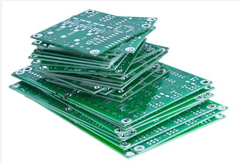
Effective PCB assembly processes rely on balancing precision, speed, and quality in SMT workflows. A well-optimized surface-mount technology line integrates automated optical inspection (AOI) systems to detect defects early, reducing rework costs and ensuring consistent PCBA outputs. Prioritizing precision component placement minimizes misalignment risks, while advanced reflow soldering profiles maintain solder joint integrity across varying thermal conditions.
Tip: For high-volume production, consider modular SMT equipment that allows rapid changeovers between product batches without compromising placement accuracy.
Integrating pick-and-place robotics with real-time monitoring software enhances throughput in PCB manufacturing, particularly when paired with predictive maintenance protocols. Manufacturers should also leverage statistical process control (SPC) tools to track key metrics like first-pass yield and cycle times, enabling data-driven adjustments. For specialized applications, partnering with experienced PCBA service providers ensures access to cutting-edge SMT assembly capabilities while maintaining compliance with industry standards.
By harmonizing automated inspection with flexible process design, electronics producers can achieve 20-35% efficiency gains in SMT workflows without sacrificing reliability—a critical advantage in competitive PCB assembly markets.
Streamline SMT Assembly for PCB Efficiency
Achieving optimal efficiency in PCB assembly requires strategic refinement of SMT (Surface Mount Technology) workflows. Modern PCBA (Printed Circuit Board Assembly) processes benefit from synchronized equipment calibration, where high-speed pick-and-place machines align components with micron-level accuracy. Integrating real-time process monitoring ensures consistent solder paste deposition, reducing defects during reflow soldering. Manufacturers leveraging closed-loop feedback systems can dynamically adjust thermal profiles, minimizing voids while maintaining cycle times.
A critical focus lies in minimizing material waste through tape-and-reel optimization and feeder slot utilization, which directly impacts throughput in high-volume production. Advanced SMT assembly lines now employ machine learning algorithms to predict placement errors before they occur, enabling preemptive corrections. Transitioning to modular workstation designs further enhances flexibility, allowing rapid reconfiguration for mixed-product batches without sacrificing precision.
By aligning equipment capabilities with design-for-manufacturing (DFM) principles, engineers can reduce rework rates by up to 40% in PCBA projects. This systemic approach not shortens time-to-market but ensures compliance with IPC-A-610 standards, creating a foundation for scalable, cost-effective electronics manufacturing.
Precision Component Placement in SMT
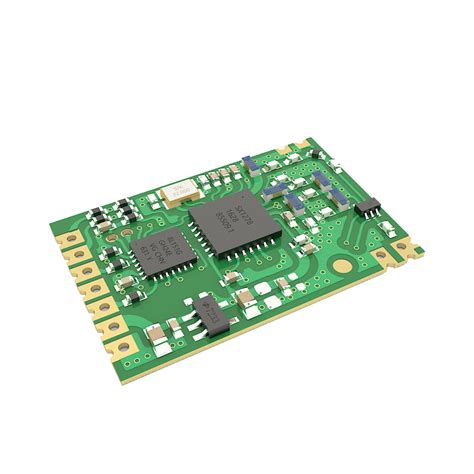
Achieving precision component placement in SMT (Surface Mount Technology) processes is foundational to successful PCB assembly and PCBA (Printed Circuit Board Assembly). Modern pick-and-place systems, such as high-speed modular platforms, leverage advanced vision systems and real-time feedback mechanisms to position components with micron-level accuracy. This ensures even ultra-fine-pitch devices, such as 0.3mm microBGAs or 01005 resistors, align perfectly with their designated pads.
Critical factors influencing placement accuracy include:
| Factor | Impact |
|---|---|
| Component Size | Smaller parts require higher nozzle precision and lighting calibration. |
| Pad Design | Optimized pad geometry minimizes tombstoning or misalignment risks. |
| Thermal Management | Stable ambient conditions prevent warping during placement. |
To maintain consistency, manufacturers integrate closed-loop calibration systems that adjust for variances in tape feeders or board flex. Additionally, dynamic fiducial recognition compensates for panel warpage, ensuring repeatability across high-volume PCBA runs. By refining these parameters, assembly lines reduce rework rates and enhance throughput, directly supporting downstream processes like reflow soldering. This alignment between precision and efficiency underscores why meticulous component placement remains a cornerstone of modern PCB assembly workflows.
Optimizing Reflow Soldering Techniques
Effective reflow soldering remains a critical phase in PCB assembly, directly impacting both yield rates and long-term reliability in PCBA manufacturing. Achieving optimal results requires precise control of thermal profiles, which govern the temperature gradients during preheating, soaking, and cooling stages. Excessive ramp rates can induce thermal stress, while insufficient peak temperatures may lead to incomplete solder joint formation. Modern systems leverage closed-loop thermal management to dynamically adjust heating zones, ensuring uniform heat distribution across complex board layouts.
The selection of solder paste alloys also plays a pivotal role, with low-void formulations minimizing defects like bridging or tombstoning. Implementing nitrogen-assisted reflow environments further reduces oxidation risks, particularly for fine-pitch components. Post-reflow, inline automated optical inspection (AOI) systems validate joint integrity, creating a seamless transition to subsequent quality control stages. By integrating real-time data analytics, manufacturers can correlate profile adjustments with defect patterns, enabling continuous process refinement.
To balance throughput and precision, advanced reflow ovens now feature modular designs, allowing rapid configuration changes for mixed-product batches. This adaptability is essential for high-mix PCBA production, where varying component densities demand tailored thermal strategies. Pairing these innovations with rigorous operator training ensures consistent outcomes, reinforcing the connection between optimized reflow techniques and overall assembly efficiency.
Automated Inspection for PCB Quality Control
Modern PCB assembly workflows rely heavily on automated inspection systems to ensure consistent quality in PCBA manufacturing. Advanced tools like Automated Optical Inspection (AOI) and X-ray inspection scan solder joints, component alignment, and hidden connections with micron-level precision, identifying defects such as bridging, tombstoning, or insufficient solder paste. By integrating these systems directly into SMT assembly lines, manufacturers achieve real-time feedback, reducing manual rework and minimizing production delays.
Machine learning algorithms further enhance defect detection accuracy, analyzing thousands of boards to refine inspection criteria dynamically. For high-density designs, 3D SPI (Solder Paste Inspection) systems preemptively verify paste volume and placement before component mounting, preventing costly errors downstream. This layered approach not only streamlines PCBA validation but also aligns with industry benchmarks like IPC-A-610, ensuring compliance without compromising throughput. As PCB assembly scales toward smaller components and tighter tolerances, automated inspection remains indispensable for balancing speed and reliability in electronics manufacturing.
Enhancing SMT Efficiency via Automation
Modern PCB assembly workflows increasingly rely on automation to address the complexities of high-density designs and shrinking component sizes. Automated pick-and-place systems, integrated with machine vision, achieve sub-micron accuracy in component positioning, reducing placement errors by over 60% compared to manual methods. These systems synchronize with PCBA production lines, enabling continuous material feeding and minimizing downtime between batches. Advanced conveyor systems and robotic handlers further streamline workflows, ensuring consistent throughput even for mixed-product batches.
Real-time process monitoring, powered by IoT-enabled sensors, allows manufacturers to detect anomalies in solder paste deposition or reflow profiles before defects occur. Closed-loop feedback mechanisms automatically adjust parameters like nozzle pressure or oven temperatures, maintaining process stability across extended production runs. For quality assurance, automated optical inspection (AOI) systems equipped with AI algorithms identify soldering defects or misaligned components at speeds exceeding 20,000 inspections per hour. By integrating these technologies, manufacturers achieve a 30–40% reduction in cycle times while sustaining defect rates below 50 ppm.
To explore advanced automation strategies for PCB assembly, refer to industry-leading methodologies that balance scalability with precision. This approach ensures PCBA lines meet evolving demands for miniaturization and high-volume output without compromising reliability.
Key Techniques for Modern SMT Assembly
Central to achieving high-performance PCB assembly is the integration of advanced SMT assembly methodologies. Precision begins with vision-guided pick-and-place systems, which ensure micron-level accuracy for components as small as 01005 packages. These systems leverage real-time feedback to adjust placement parameters, minimizing misalignment risks. Equally critical is stencil printing optimization, where solder paste volume consistency directly impacts joint reliability. Advanced systems employ laser-cut stencils with nano-coated surfaces to reduce clogging and improve deposition uniformity.
Another pivotal technique involves dynamic reflow soldering profiles tailored to specific PCBA designs. By analyzing thermal mass variations across the board, engineers can create multi-zone temperature curves that prevent tombstoning or solder bridging. Pairing this with nitrogen-enriched reflow ovens further enhances wetting performance while reducing oxidation.
Modern facilities also prioritize automated optical inspection (AOI) paired with machine learning algorithms. These systems detect defects like insufficient solder or skewed components at speeds exceeding 20,000 inspections per hour, ensuring compliance with IPC-A-610 standards. Furthermore, closed-loop feedback mechanisms link inspection data directly to placement machines, enabling self-correction in real time.
To maintain throughput, lean material handling practices—such as smart feeder setups and tape-and-reel optimization—minimize machine idle periods. By synchronizing these techniques, manufacturers achieve the delicate balance of scaling SMT assembly output without compromising the integrity of PCB assembly outcomes.
Balancing Speed and Quality in PCB Production
Achieving optimal efficiency in PCB assembly requires a delicate equilibrium between throughput and reliability. While faster production cycles reduce lead times, compromising on quality risks costly rework or field failures. Modern surface-mount technology (SMT) lines address this challenge through adaptive process controls and real-time monitoring systems. For instance, integrating PCBA-specific thermal profiling ensures consistent solder joint integrity across high-speed reflow ovens, even during rapid heating cycles. Advanced pick-and-place systems equipped with vision-guided alignment maintain micron-level accuracy at speeds exceeding 40,000 components per hour.
To sustain this balance, manufacturers employ closed-loop feedback mechanisms, such as inline automated optical inspection (AOI), which scans boards post-reflow without interrupting the conveyor flow. This dual focus on velocity and verification reduces defect escape rates by 60% compared to traditional sampling methods. Additionally, modular PCB assembly workflows allow simultaneous optimization of individual stages—like stencil printing or component placement—without destabilizing the entire line. By aligning machine calibration with design-for-manufacturability (DFM) principles, PCBA providers achieve <2% process variation while maintaining cycle times under 90 seconds per board, proving that speed and quality in electronics manufacturing are not mutually exclusive goals.
Advanced SMT Methods for Reliable Electronics
Modern PCB assembly processes demand advanced SMT techniques to ensure long-term reliability in electronic devices. By integrating high-resolution stencil printing with laser-aligned pick-and-place systems, manufacturers achieve micron-level accuracy in component positioning—critical for densely packed PCBA designs. The adoption of nitrogen-assisted reflow ovens minimizes oxidation during soldering, reducing defects like void formation or cold joints. For mission-critical applications, 3D solder paste inspection (SPI) systems paired with automated optical inspection (AOI) create a closed-loop feedback mechanism, identifying deviations in real time and enabling immediate process adjustments.
Emerging methods such as predictive thermal profiling leverage machine learning to optimize reflow parameters dynamically, accounting for variations in PCB assembly materials or environmental conditions. Additionally, the use of low-voiding solder pastes combined with precision underfill dispensing enhances mechanical stability in high-vibration environments. These innovations not only improve yield rates but also extend the operational lifespan of PCBA units, aligning with industry demands for both performance and durability. Transitioning to such methodologies ensures seamless compatibility with next-generation electronics, where reliability is non-negotiable.

Conclusion
The evolution of PCB assembly processes hinges on harmonizing precision, speed, and reliability in SMT workflows. By integrating advanced automated inspection systems and refining reflow soldering profiles, manufacturers can achieve consistent quality in PCBA outputs while scaling production throughput. A critical factor lies in leveraging data-driven insights to fine-tune component placement accuracy, reducing defects that compromise yield rates.
Adopting modular automation frameworks—such as inline solder paste inspection (SPI) and automated optical inspection (AOI)—ensures real-time feedback loops, enabling rapid adjustments during PCB assembly. For instance, optimizing thermal management during reflow phases minimizes solder bridging, a common challenge in high-density PCBA designs. Additionally, aligning SMT workflows with design-for-manufacturing (DFM) principles streamlines transitions from prototyping to mass production.
To deepen these strategies, manufacturers should reference industry-proven methodologies for SMT process optimization. Ultimately, the synergy between precision engineering and intelligent automation positions PCB assembly lines to meet escalating demands for miniaturized, high-performance electronics—without sacrificing reliability or cost-efficiency.
Frequently Asked Questions
What distinguishes SMT from traditional through-hole assembly in PCB assembly?
Surface-mount technology (SMT) enables direct placement of components onto the PCB surface, eliminating the need for drilled holes. This reduces material waste and allows higher component density compared to through-hole methods, making PCBA processes faster and more scalable.
How does reflow soldering impact PCB assembly quality?
Reflow soldering precision ensures consistent solder joint formation, critical for electrical reliability. Optimizing temperature profiles minimizes defects like tombstoning or bridging, directly affecting yield rates in PCBA workflows.
Why is automated inspection vital in modern SMT lines?
Automated optical inspection (AOI) and X-ray systems detect micron-level defects, such as misaligned components or insufficient solder. These tools reduce human error and align with industry standards for high-volume PCB assembly environments.
Can automation compromise flexibility in PCBA production?
Advanced modular systems balance speed with adaptability. Programmable pick-and-place machines and AI-driven inspection adapt to design changes without sacrificing throughput, ensuring efficient PCB assembly even for mixed-batch orders.
What factors determine the cost-efficiency of SMT processes?
Key drivers include component placement accuracy, solder paste utilization, and defect rates. Implementing lean principles in PCBA workflows—such as minimizing rework cycles—directly lowers operational costs while maintaining quality.
Ready to Optimize Your PCB Assembly Workflow?
For tailored solutions in PCB assembly and PCBA optimization, please click here to connect with industry experts and elevate your manufacturing efficiency.