Optimizing SMT PCB Assembly for High-Density Electronics

Key Takeaways
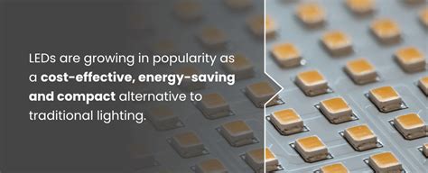
Effective PCB assembly processes for high-density electronics require meticulous attention to precision and material compatibility. Central to PCBA success is the integration of precision component placement, which minimizes errors in densely packed layouts. Optimizing solder paste application ensures reliable electrical connections, particularly for miniaturized components where even micron-level deviations can impact performance. Equally critical is addressing thermal management through strategic material choices and layout designs that dissipate heat efficiently, preventing overheating in compact configurations.
The selection of high-performance substrates and low-void solder pastes enhances durability, while advanced stenciling techniques improve paste deposition accuracy. Automated optical inspection (AOI) systems play a pivotal role in maintaining quality, detecting defects early in the PCB assembly workflow. As PCBA technology evolves, trends like embedded components and AI-driven process optimization are reshaping high-density manufacturing, offering pathways to further reliability and scalability. These strategies collectively address the unique challenges of modern electronics, balancing miniaturization with robust functionality.
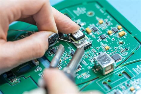
Precision SMT Component Placement Techniques
Achieving optimal performance in high-density PCB assembly begins with mastering precision component placement. Modern SMT (Surface Mount Technology) processes rely on advanced pick-and-place systems equipped with vision-guided robotics to position components as small as 01005 packages (0.4mm x 0.2mm) with micron-level accuracy. Critical factors such as nozzle selection, feeder calibration, and machine vibration control directly influence placement repeatability, especially for miniaturized PCBA designs.
To mitigate misalignment risks, engineers employ fiducial markers and 3D solder paste inspection (SPI) to ensure consistent reference points before placement. For ultra-fine-pitch components like 0.4mm-pitch BGAs or QFNs, dynamic lighting adjustments and thermal compensation algorithms help maintain positional integrity across varying environmental conditions. Additionally, optimizing feeder tape tension and vacuum pressure settings reduces tombstoning and skewing defects in high-density PCB assemblies.
A key challenge lies in balancing speed and precision. While high-speed placers achieve rates exceeding 30,000 components per hour, delicate parts such as MEMS sensors or RF modules often require hybrid systems combining modular gantries with ultra-precision servo motors. Integrating real-time feedback loops via machine learning further refines placement accuracy by analyzing historical process data to predict and correct deviations.
Finally, collaboration between PCB assembly teams and design engineers ensures component footprints and pad geometries align with stencil apertures and reflow profiles—a synergy critical for avoiding solder bridging or voiding in densely packed layouts. This alignment becomes especially vital as industries push toward 5G and IoT devices, where millimeter-scale tolerances define functional reliability.
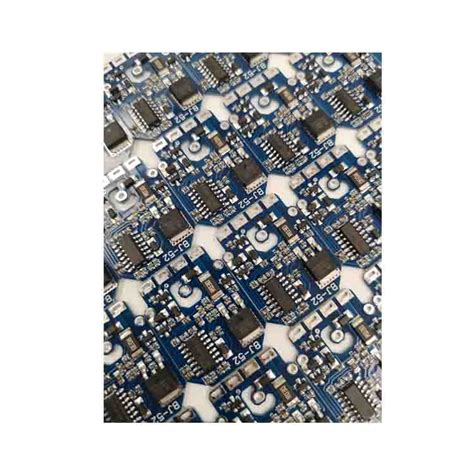
Solder Paste Optimization for Miniaturized PCBs
Effective PCB assembly of high-density electronics demands meticulous attention to solder paste application, particularly as component sizes shrink below 01005 metrics. In PCBA processes, achieving reliable solder joints in miniaturized layouts requires balancing viscosity, metal content, and particle size distribution. Advanced solder paste formulations with Type 5 or Type 6 powder (particle sizes 15-25 μm) enable finer deposition, critical for micro-BGA packages and 0.3mm pitch QFNs.
Stencil design plays a pivotal role, with laser-cut apertures and electroformed nickel templates ensuring precise paste transfer for ultra-fine traces. A step-stencil approach, combining 80μm thickness for passive components and 50μm for ICs, optimizes volume control without compromising print speed. For high-mix PCB assembly lines, dynamic temperature profiling during reflow prevents tombstoning or bridging, while nitrogen-enriched environments reduce oxidation risks.
Automated optical inspection (AOI) systems now integrate AI-driven algorithms to detect sub-25μm defects, such as insufficient paste or misalignment. Pairing these tools with real-time viscosity monitoring in stencil printers ensures consistent performance across PCBA batches. As component densities increase, optimizing these parameters becomes essential for maintaining yield rates above 99.95% in mission-critical applications like medical implants or aerospace systems. This precision directly supports subsequent thermal management strategies by minimizing voiding and ensuring uniform heat dissipation paths.
Thermal Management in High-Density PCB Designs
Effective thermal management remains critical in PCB assembly for high-density electronics, where component miniaturization and increased power density create significant heat dissipation challenges. Thermal resistance reduction begins with material selection—using substrates with high thermal conductivity, such as metal-core or ceramic-filled laminates, to improve heat transfer. PCBA designs often incorporate thermal vias beneath high-power components, creating conductive pathways to distribute heat toward inner layers or external heatsinks.
A balanced approach combines passive and active cooling strategies:
| Technique | Application | Benefit |
|---|---|---|
| Embedded heat spreaders | High-power ICs/RF modules | Localized heat redistribution |
| Thermal interface pads | Between components and chassis | Improved conduction to external sinks |
| Forced air cooling | Enclosed systems with limited airflow | Enhanced convective heat removal |
In ultra-compact layouts, thermal simulation tools are indispensable for predicting hot spots and optimizing component placement during PCB assembly. Designers must also account for coefficient of thermal expansion (CTE) mismatches, which can induce mechanical stress in solder joints during thermal cycling. Proactive management of these factors ensures long-term reliability in PCBA systems, particularly in applications like automotive electronics or IoT devices where operational temperatures fluctuate widely. This integration of thermal strategies aligns with broader objectives for high-density PCB assembly, enabling performance stability without compromising spatial efficiency.
Enhancing Reliability in Compact SMT Assemblies
Achieving long-term reliability in PCB assembly for high-density electronics demands meticulous attention to material compatibility, process control, and environmental stressors. As component sizes shrink and interconnects tighten in PCBA designs, thermal cycling and mechanical strain become critical failure points. Engineers address these challenges by selecting substrates with low coefficient of thermal expansion (CTE) to minimize stress during temperature fluctuations. Advanced underfill materials are applied to reinforce solder joints in ball grid arrays (BGAs) and chip-scale packages (CSPs), preventing microcracks caused by vibration or thermal fatigue.
Process optimization plays an equally vital role. Strict adherence to reflow profiles ensures proper wetting of ultra-fine-pitch components while avoiding tombstoning or solder bridging. Conformal coatings with high dielectric strength protect densely packed circuits from moisture ingress and contamination—a common risk in compact designs. For mission-critical applications, accelerated life testing simulates years of operational stress within weeks, validating design choices under extreme conditions.
Transitioning to the next phase, these reliability-focused strategies directly support the implementation of automated inspection systems, which will be explored in subsequent sections. By integrating robust materials, precise process controls, and rigorous testing protocols, manufacturers can deliver PCB assembly solutions that meet the stringent demands of modern high-density electronics.
Advanced Stenciling Methods for SMT Efficiency
Effective PCB assembly relies heavily on precision stenciling to ensure consistent solder paste deposition, particularly in high-density PCBA applications. Modern laser-cut stencils with electropolished apertures minimize paste clogging, enabling accurate transfer for components as small as 01005 packages. To address challenges in ultra-fine-pitch designs, step stencils with varying thicknesses optimize paste volume across mixed-component layouts, reducing bridging risks while maintaining joint integrity. Advanced nano-coated stencils further enhance solder release efficiency, cutting downtime for cleaning by up to 40% in high-volume production.
For complex SMT PCB board designs, 3D-printed stencils enable customized aperture geometries, aligning with irregular pad shapes or tight clearances. Real-time solder paste inspection (SPI) systems integrated with stencil printers validate deposition quality, ensuring <10% deviation in paste volume. By combining these methods with dynamic squeegee pressure control, manufacturers achieve first-pass yields exceeding 99.2%, even in assemblies with 0.3mm pitch BGAs. Such innovations not only accelerate throughput but also reduce rework costs, making them critical for next-generation PCBA workflows demanding micron-level precision.
Material Selection for Durable SMT PCB Boards
The longevity and performance of SMT PCB assemblies hinge on strategic material choices that balance electrical, thermal, and mechanical demands. For high-density designs, substrate materials like FR-4 with high glass transition temperatures (Tg > 170°C) or specialized laminates such as polyimide or Rogers substrates are critical to withstand repeated thermal cycling during PCBA processes. Copper weight and trace thickness must align with current-carrying requirements while minimizing impedance mismatches.
Tip: When selecting solder mask materials, opt for liquid photoimageable (LPI) types with excellent adhesion and thermal resistance to prevent delamination in compact layouts.
Dielectric properties play a pivotal role in signal integrity, particularly for high-frequency applications. Materials with low dielectric loss (Df < 0.005) and stable permittivity (Dk) across temperature variations reduce signal attenuation in densely routed boards. For components exposed to mechanical stress, such as connectors or large BGAs, reinforced substrates or metal-core PCBs enhance structural stability.
Surface finishes like ENIG (Electroless Nickel Immersion Gold) or immersion silver provide reliable solderability for fine-pitch components, while conformal coatings protect against environmental factors. Compatibility between materials—such as matching the coefficient of thermal expansion (CTE) of substrates and copper layers—prevents warping and via cracking during reflow. By prioritizing material synergy, manufacturers ensure PCB assemblies meet both miniaturization goals and long-term reliability standards in demanding applications.
Automated Inspection in High-Density Electronics
Modern PCB assembly processes demand rigorous quality control, particularly in high-density electronics where component spacing often falls below 100 microns. Automated optical inspection (AOI) systems have become indispensable for identifying defects like solder bridging, misaligned components, or insufficient paste volume in PCBA workflows. These systems employ high-resolution cameras and machine learning algorithms to analyze thousands of solder joints per minute, achieving defect detection rates exceeding 99.5% in optimized setups. For hidden interconnects or ball grid array (BGA) components, X-ray inspection complements AOI by verifying subsurface connections without disassembly—a critical capability for multi-layer designs.
Advanced PCB assembly lines now integrate inspection data with process controls, enabling real-time adjustments to stencil printing or reflow parameters. This closed-loop approach minimizes rework cycles while maintaining yield efficiency in PCBA production. As component miniaturization accelerates, emerging techniques like 3D solder paste inspection (SPI) and AI-powered anomaly prediction are reshaping quality assurance frameworks. These innovations not only address current challenges in high-density electronics but also lay the groundwork for next-generation assembly standards, ensuring reliability as feature sizes approach physical limits.
Future Trends in SMT PCB Assembly Technology
As high-density electronics evolve, PCB assembly processes are adapting to meet demands for greater precision and scalability. Emerging technologies like AI-driven placement systems and adaptive solder paste dispensing are redefining PCBA workflows, enabling faster production cycles while maintaining micron-level accuracy. The integration of additive manufacturing for custom stencils allows finer control over solder deposition, critical for ultra-compact SMT PCB boards with 0201 or 01005 components.
Another key development lies in thermally conductive substrates that address heat dissipation challenges in densely packed designs, complementing advancements in laser-assisted reflow soldering. Industry 4.0 adoption is accelerating, with IoT-enabled assembly lines providing real-time analytics to optimize PCB assembly yields. Additionally, sustainable practices are gaining traction, including halogen-free laminates and recyclable solder alloys, aligning with global environmental standards.
Looking ahead, heterogeneous integration techniques will likely dominate, merging PCBA with embedded active/passive components to reduce footprint and improve signal integrity. Collaborative robotics and digital twin simulations are poised to further refine process validation, ensuring reliability in next-generation high-density applications. These innovations collectively signal a shift toward smarter, more resilient manufacturing ecosystems for advanced electronics.
Conclusion
The evolution of SMT PCB assembly processes underscores the critical balance between precision, material science, and thermal dynamics in modern high-density electronics. As demand for compact, high-performance devices grows, optimizing PCBA workflows requires integrating advanced techniques like laser-cut stenciling, nano-coated solder pastes, and real-time automated inspection systems. These innovations not only address challenges in miniaturization but also ensure long-term reliability under extreme operating conditions.
Looking ahead, the adoption of AI-driven placement algorithms and thermally conductive substrate materials will further refine PCB assembly efficiency. However, success hinges on aligning these advancements with rigorous testing protocols and sustainable manufacturing practices. By prioritizing design-for-manufacturability principles, engineers can mitigate risks in PCBA while meeting the escalating demands of IoT, wearables, and 5G infrastructure. The future of SMT technology lies in harmonizing cutting-edge methodologies with cost-effective scalability—a paradigm shift that continues to redefine the boundaries of electronic miniaturization.
Frequently Asked Questions
What distinguishes high-density PCB assembly from traditional methods?
High-density PCBA requires specialized techniques like microscopic component placement and advanced solder paste formulations to accommodate miniaturized layouts. Unlike conventional assemblies, it prioritizes thermal dissipation and signal integrity in tightly packed designs.
How does solder paste optimization improve reliability in PCB assembly?
Precisely engineered solder pastes with fine particle sizes ensure consistent deposition for ultra-small components. This reduces voiding and bridging risks, critical for achieving robust electrical connections in high-density PCBA.
What role does material selection play in compact SMT PCB boards?
High-performance substrates with low thermal expansion and enhanced dielectric properties minimize warping and signal loss. Materials like polyimide or ceramic-filled laminates are often chosen for durable PCB assemblies in demanding environments.
Can automated inspection systems handle high-density component arrays?
Modern 3D AOI (Automated Optical Inspection) systems detect defects as small as 01005 passives, ensuring accuracy in PCB assembly. Combined with X-ray inspection, they verify solder joints under BGAs or QFN packages invisible to traditional methods.
Why is thermal management critical for high-density PCBA longevity?
Concentrated heat in compact designs accelerates component degradation. Techniques like embedded copper heatsinks and thermal vias dissipate heat efficiently, preventing premature failure in SMT PCB boards.
Ready to Optimize Your SMT Process?
For tailored solutions in high-density PCB assembly, please click here to consult our engineering team.