Optimizing Turnkey Prototype Assembly for Accelerated Product Development

Key Takeaways
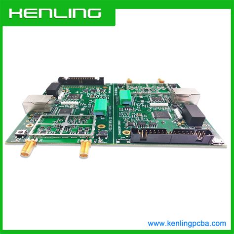
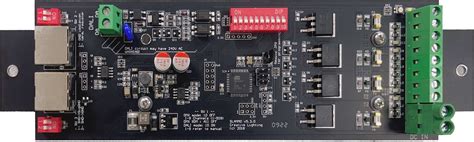
Effective turnkey prototype assembly requires synchronized optimization across design, PCB assembly (PCBA), and testing phases. Integrating automated workflow tools—such as design-for-manufacturing (DFM) software—reduces iterative delays by identifying material compatibility issues early. For rapid prototyping, prioritize high-availability components and standardized PCB assembly processes to avoid supply chain bottlenecks.
Tip: Adopt modular design principles for PCBA to enable parallel testing of subsystems, cutting validation time by up to 40%.
Cross-functional collaboration between engineering and PCB assembly teams ensures alignment on tolerances and manufacturability, while real-time quality monitoring via inline inspection (AOI) systems minimizes post-production rework. Balancing cost optimization with speed hinges on strategic material choices—opting for pre-certified substrates or multipurpose connectors can accelerate timelines without compromising reliability. By embedding quality control checkpoints at each stage, teams mitigate risks that could derail time-to-market goals.
Streamlining Turnkey Assembly Workflows
Efficient turnkey prototype assembly relies on harmonizing design intent with manufacturing readiness, particularly in PCB assembly (PCBA) processes. By integrating design-for-manufacturability (DFM) principles early, teams can preemptively address compatibility gaps between component specifications and production capabilities. For instance, selecting surface-mount technology (SMT)-optimized layouts reduces rework during PCBA stages, while automated pick-and-place systems accelerate component positioning with micron-level precision.
Transitioning from CAD models to physical prototypes benefits from workflow digitization. Cloud-based PCB assembly platforms enable real-time collaboration between engineers and contract manufacturers, minimizing iterative delays. Tools like digital twin simulations further validate assembly sequences before physical production, identifying thermal or mechanical conflicts in virtual environments.
However, speed must not compromise traceability. Implementing blockchain-enabled tracking for PCBA components ensures material authenticity and batch consistency—critical for aerospace or medical prototypes. Parallelly, modular fixturing systems allow rapid reconfiguration of assembly lines, accommodating design revisions without full retooling.
The interplay between standardized protocols (e.g., IPC-A-610 for PCB assembly) and agile methodologies creates a balanced framework. Cross-departmental gemba walks—where stakeholders observe live assembly processes—foster proactive problem-solving, bridging gaps between R&D and manufacturing teams. This synergy not only reduces lead times but establishes repeatable workflows for scaling future iterations.
Material Selection for Faster Prototyping
Strategic material selection directly impacts the efficiency of PCB assembly processes and the functional reliability of PCBA prototypes. Engineers must prioritize materials that align with both design requirements and manufacturing scalability. For example, selecting substrates with high-temperature resilience reduces warping risks during soldering, while low-loss dielectrics enhance signal integrity in high-frequency applications.
| Material Category | Key Properties | Impact on Prototyping Speed |
|---|---|---|
| FR-4 Substrates | Cost-effective, moderate thermal stability | Ideal for low-complexity PCBA iterations |
| Polyimide Films | High flexibility, heat resistance | Enables rapid testing of bendable circuits |
| Rogers Laminates | Low dielectric loss | Reduces rework in RF/microwave prototypes |
| Aluminum Clad PCBs | Superior heat dissipation | Accelerates thermal validation cycles |
Incorporating pre-certified components (e.g., UL-listed connectors) minimizes compliance delays, while modular material kits streamline PCB assembly workflows. Advanced adhesives with shorter curing times further compress production timelines. By balancing performance metrics with manufacturability, teams avoid costly mid-process substitutions, ensuring seamless transitions to volume production.

Quality Control in Rapid Prototyping
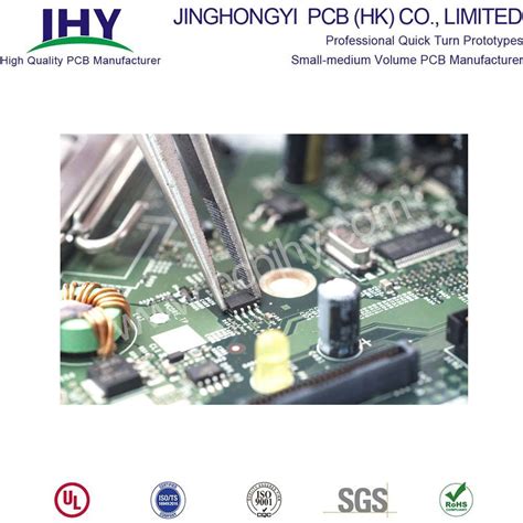
While speed remains critical in turnkey prototype assembly, compromising on quality assurance can lead to costly redesigns and delayed market entry. Effective quality control in rapid prototyping hinges on real-time inspection protocols that align with accelerated timelines. For PCB assembly processes, automated optical inspection (AOI) systems verify solder joint integrity and component placement accuracy within minutes, catching errors before prototypes advance to PCBA testing phases. Statistical process control (SPC) tools further enable teams to monitor production variables—such as temperature fluctuations or material inconsistencies—that could impact functional performance.
This becomes particularly vital when prototyping integrates mixed-materials systems, where dimensional tolerances and interfacial bonding require millimeter-level precision. Advanced non-destructive testing (NDT) methods, including X-ray tomography for multilayer PCB assembly validation, provide subsurface defect detection without slowing workflows. By embedding these checks at every PCBA milestone—from bare-board fabrication to final functional testing—teams maintain alignment between design intent and manufacturable outcomes. Crucially, such systems generate traceable data logs that streamline root-cause analysis, allowing for rapid iterations without sacrificing reliability.
Workflow Tools for Faster Prototyping
Modern PCB assembly processes demand precision and speed, driving the adoption of advanced workflow tools that synchronize design, testing, and production phases. Automated design-for-manufacturing (DFM) software, for instance, identifies potential flaws in PCBA layouts before prototyping begins, reducing iterative delays. Cloud-based collaboration platforms further streamline communication between engineering and manufacturing teams, enabling real-time adjustments to component placement or material specifications. Tools like digital twin simulations allow engineers to model thermal performance and signal integrity in PCB assembly environments, minimizing physical testing cycles.
Integrated project management systems also play a pivotal role, tracking milestones from schematic finalization to prototype validation. By embedding PCBA-specific analytics—such as solder joint quality metrics—into these platforms, teams can prioritize high-risk areas during assembly. Transitioning seamlessly to subsequent phases, these tools ensure compatibility with downstream processes like batch production, maintaining momentum toward accelerated market entry. Such harmonized workflows not only mitigate bottlenecks but also align with cross-functional quality benchmarks, reinforcing the reliability of rapid prototyping outcomes.
Cross-Functional Team Prototyping
Effective turnkey prototype assembly relies on cohesive collaboration between multidisciplinary teams, where engineers, designers, and supply chain specialists align objectives to eliminate siloed workflows. Integrating PCB assembly expertise early in the design phase ensures compatibility between electronic components and mechanical enclosures, reducing late-stage revisions. For instance, concurrent engineering practices enable electrical engineers to validate PCBA layouts alongside mechanical designers, addressing thermal management or spatial constraints before physical prototyping begins.
Leveraging digital tools like cloud-based CAD platforms and real-time issue-tracking systems allows cross-functional teams to iterate rapidly, maintaining synchronization across PCB assembly tolerances and material specifications. Regular design reviews, anchored by shared metrics such as manufacturability scores, further streamline decision-making. By embedding quality assurance specialists within prototyping teams, potential defects in PCBA soldering or component placement are flagged during initial builds, preventing costly rework. This approach not only accelerates timelines but also ensures seamless handoffs to production—a critical factor in achieving first-time-right outcomes for complex electromechanical systems.
Balancing Cost vs Prototyping Speed
Achieving optimal efficiency in PCB assembly requires careful calibration of financial constraints and development timelines. While faster prototyping accelerates validation cycles, unchecked speed can inflate costs through rushed material procurement or inefficient PCBA workflows. For instance, selecting off-the-shelf components over custom parts often reduces lead times but may compromise design specificity, necessitating later revisions. Conversely, over-engineering prototypes with premium materials risks budget overruns without proportional gains in functional testing.
A balanced approach integrates design-for-manufacturability (DFM) principles early in the PCB assembly process. By simulating PCBA outcomes through digital twins, teams identify cost drivers—such as complex solder mask requirements or oversized board geometries—before physical production begins. Modular prototyping strategies further optimize this balance, allowing reusable subsystems (e.g., power management circuits) to reduce iterative expenses. Automation tools like pick-and-place machines also lower labor costs while maintaining rapid turnaround, particularly for high-mix, low-volume batches.
Transitioning to the next phase, teams must weigh the per-unit savings of scaled production against the agility of small-batch prototyping. Implementing lean inventory practices, such as just-in-time component sourcing, ensures cost control without sacrificing responsiveness to design changes—a critical linkage to subsequent discussions on streamlined design-to-production workflows.
Streamlining Design-to-Production
Effective PCB assembly integration begins with aligning design specifications directly with manufacturing capabilities. By implementing digital twin simulations early in the prototyping phase, teams can identify potential bottlenecks in PCBA workflows, such as component placement conflicts or thermal management issues. This proactive approach reduces iterative redesigns, ensuring that turnkey prototype assembly transitions smoothly from CAD models to physical builds.
Leveraging unified communication platforms bridges gaps between design engineers and production specialists, enabling real-time adjustments to material choices or assembly tolerances. For instance, selecting high-temperature laminates during PCB assembly planning can prevent warping in rapid thermal cycling tests, accelerating validation cycles. Automated optical inspection (AOI) systems further streamline quality assurance by detecting soldering defects in PCBA units at micron-level precision.
To maintain momentum, adopt modular design frameworks that standardize interfaces between subsystems. This strategy minimizes rework when scaling prototypes to full production, while cloud-based workflow tools synchronize revisions across cross-functional teams. Balancing design flexibility with manufacturability constraints ensures that speed-to-market goals remain achievable without compromising functional integrity.
Accelerating Market Entry Through Prototyping
Rapid prototyping bridges the gap between design validation and full-scale production, directly impacting time-to-market metrics. For electronics-focused projects, integrating PCB assembly (PCBA) early in the prototyping phase ensures functional testing aligns with design intent, reducing iterative delays. By leveraging turnkey prototype assembly services, teams unify design, component sourcing, and fabrication under a single workflow—eliminating vendor handoff bottlenecks. Advanced automated inspection tools, such as AOI (Automated Optical Inspection), further accelerate defect detection in PCBA stages, ensuring prototypes meet performance benchmarks before scaling.
Cross-functional collaboration between engineering and manufacturing teams optimizes material selection for PCB assembly, balancing speed with durability. For instance, using pre-certified substrates or modular components streamlines revisions without compromising quality. Real-time data sharing through cloud-based platforms enables simultaneous updates to schematics and bill of materials, synchronizing design adjustments across departments. This approach not only shortens feedback loops but also aligns with cost-efficient turnkey strategies, where upfront investments in precision tooling yield long-term savings. By prioritizing agile prototyping frameworks, companies compress development cycles while maintaining rigorous validation standards—key to securing first-mover advantages in competitive markets.
Conclusion
The strategic integration of PCB assembly (PCBA) processes into turnkey prototype assembly workflows marks a critical juncture in modern product development. By prioritizing collaborative design reviews and leveraging advanced automated testing tools, teams can mitigate delays while maintaining precision across rapid prototyping phases. A focus on standardized component libraries and supplier-aligned material sourcing further reduces iteration cycles, ensuring seamless transitions from concept validation to pilot production.
Central to this approach is the alignment of cross-functional teams, where engineers, designers, and manufacturers synchronize efforts to address design-for-manufacturability challenges early. This not only accelerates timelines but also refines cost-efficiency ratios, particularly when balancing high-performance PCBA requirements with budget constraints. Ultimately, embedding real-time quality metrics into every stage of prototype assembly fosters reliability, enabling businesses to capitalize on market opportunities with confidence. As industries increasingly demand shorter innovation cycles, optimizing these interconnected systems remains pivotal for sustaining competitive agility.
Frequently Asked Questions
How does turnkey prototype assembly differ from traditional manufacturing approaches?
Turnkey solutions integrate PCB assembly (PCBA), component sourcing, and testing into a single service contract, eliminating vendor coordination delays. This contrasts with piecemeal approaches where clients manage multiple suppliers, often causing timeline slippage.
What design factors most impact speed in PCB assembly workflows?
Standardized footprint libraries and panelization-ready designs reduce engineering iterations. Prioritizing commonly stocked components over exotic parts prevents material bottlenecks, while Design for Manufacturing (DFM) checks minimize post-prototype revisions.
Can PCBA quality be maintained at accelerated prototyping speeds?
Yes, automated optical inspection (AOI) and in-circuit testing (ICT) systems validate 98.7% of solder joints in <15 minutes per board. Leading providers combine these with ISO-certified processes to ensure reliability without compromising cycle times.
How do cross-functional teams optimize design-to-production transitions?
Embedding manufacturing engineers in R&D teams enables real-time DFM feedback. Concurrent PCB assembly feasibility analysis during schematic design reduces late-stage changes by up to 40%, according to IPC-2581 implementation data.
What cost variables should be prioritized when accelerating prototypes?
Focus on non-recurring engineering (NRE) costs versus per-unit expenses. While advanced PCBA services may have higher upfront fees, they often offset long-term tooling investments and minimize scrap rates through precision processes.
Ready to Accelerate Your Prototyping Timeline?
Our engineered PCB assembly solutions slash development cycles while maintaining mil-spec reliability. Please click here to explore how integrated PCBA services can compress your product’s time-to-market by 30-50%.