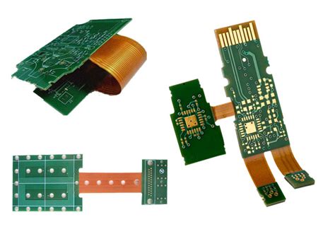
Osi pcb assembly
Understanding The OSI Model In PCB Assembly
The OSI model, or Open Systems Interconnection model, is a conceptual framework used to understand and implement network protocols in seven layers. While it is primarily associated with networking, its principles can be applied to various fields, including PCB (Printed Circuit Board) assembly. Understanding the OSI model in the context of PCB assembly can provide valuable insights into the systematic approach required for efficient and effective electronic manufacturing.
To begin with, the OSI model’s layered approach can be likened to the stages of PCB assembly, where each layer or stage has a specific function and responsibility.
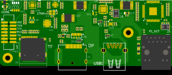
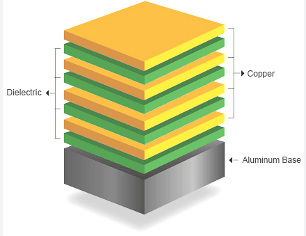
This analogy helps in visualizing the complex processes involved in PCB assembly, from design to final product testing. The first layer of the OSI model, the physical layer, corresponds to the physical aspects of PCB assembly, such as the materials used, the board’s layout, and the placement of components. This stage is crucial as it lays the foundation for the entire assembly process, much like the physical layer in networking, which deals with the transmission of raw data over a physical medium.
Moving to the second layer, the data link layer in the OSI model ensures error-free data transfer between adjacent nodes.
In PCB assembly, this can be compared to the soldering process, where components are securely attached to the board. Proper soldering techniques ensure that electrical connections are reliable and free from defects, akin to the error-checking functions of the data link layer. Transitioning to the third layer, the network layer, which is responsible for data routing, we can draw parallels to the routing of electrical signals on a PCB. This involves designing efficient pathways for electrical currents to travel between components, ensuring optimal performance and functionality.
The transport layer, the fourth in the OSI model, manages end-to-end communication and error recovery.
In PCB assembly, this can be related to the testing phase, where the assembled board is subjected to various tests to verify its functionality and identify any errors. This stage is critical for ensuring that the final product meets the required specifications and operates as intended. As we move to the fifth layer, the session layer, which establishes, manages, and terminates connections, we can see similarities in the quality control processes of PCB assembly. These processes ensure that each stage of assembly is completed correctly before moving on to the next, maintaining the integrity of the entire operation.
The presentation layer, the sixth layer of the OSI model, is responsible for data translation and encryption.
In PCB assembly, this can be likened to the final inspection and packaging of the product. This stage ensures that the assembled PCB is ready for deployment and meets all necessary standards and certifications. Finally, the application layer, which provides network services to end-users, can be compared to the deployment and integration of the PCB into its intended application. This final step ensures that the PCB functions correctly within its designated environment, much like how the application layer facilitates user interaction with network services.
In conclusion, understanding the OSI model in the context of PCB assembly offers a structured approach to the complex processes involved in electronic manufacturing. By drawing parallels between the OSI layers and the stages of PCB assembly, we can gain a deeper appreciation for the meticulous planning and execution required to produce high-quality electronic products. This systematic approach not only enhances efficiency but also ensures that each stage of the assembly process is completed with precision and accuracy.

Key Benefits Of OSI PCB Assembly For Electronics Manufacturing
In the rapidly evolving landscape of electronics manufacturing, the integration of advanced technologies and methodologies is crucial for maintaining competitive advantage. One such advancement is the OSI PCB assembly, which stands for Open Systems Interconnection Printed Circuit Board assembly. This approach offers a multitude of benefits that significantly enhance the efficiency and quality of electronics manufacturing processes. Understanding these benefits is essential for manufacturers aiming to optimize their production capabilities and deliver superior products to the market.
To begin with, OSI PCB assembly provides a standardized framework that facilitates seamless communication and interoperability between different systems and components.
This standardization is particularly beneficial in an industry characterized by a diverse array of technologies and protocols. By adhering to a common set of guidelines, manufacturers can ensure that their products are compatible with a wide range of devices and systems, thereby expanding their market reach and reducing the risk of obsolescence. Moreover, this interoperability simplifies the integration of new technologies, allowing manufacturers to quickly adapt to emerging trends and consumer demands.
In addition to enhancing compatibility, OSI PCB assembly also contributes to improved reliability and performance of electronic devices.
The structured approach to design and assembly minimizes the likelihood of errors and defects, which are common challenges in traditional manufacturing processes. By reducing these risks, manufacturers can produce high-quality products with greater consistency, thereby enhancing their reputation and customer satisfaction. Furthermore, the reliability of OSI PCB assembly translates into longer product lifespans, which is a significant advantage in a market where consumers increasingly prioritize durability and sustainability.
Another key benefit of OSI PCB assembly is its impact on cost efficiency.
The standardized processes and protocols associated with this approach streamline production, reducing the time and resources required for assembly. This efficiency not only lowers manufacturing costs but also accelerates time-to-market, enabling companies to capitalize on new opportunities more swiftly. Additionally, the reduction in errors and defects decreases the need for costly rework and repairs, further contributing to overall cost savings. These financial advantages are particularly important in an industry where margins can be tight and competition fierce.
Furthermore, OSI PCB assembly supports scalability, which is crucial for manufacturers looking to expand their operations.
The modular nature of the OSI model allows for easy adjustments and upgrades, facilitating the scaling of production to meet increasing demand. This flexibility is invaluable in a dynamic market environment, where the ability to quickly respond to changes can determine a company’s success. By adopting OSI PCB assembly, manufacturers can position themselves to grow and adapt without the need for extensive overhauls or investments in new infrastructure.
Finally, the adoption of OSI PCB assembly aligns with the growing emphasis on sustainability in electronics manufacturing.
The efficiency and reliability of this approach contribute to reduced waste and energy consumption, supporting environmentally responsible production practices. As consumers and regulatory bodies increasingly prioritize sustainability, manufacturers that embrace OSI PCB assembly can enhance their brand image and comply with evolving environmental standards.
In conclusion, OSI PCB assembly offers a comprehensive suite of benefits that are instrumental in advancing electronics manufacturing. From improved compatibility and reliability to cost efficiency and scalability, this approach addresses many of the challenges faced by manufacturers today. By leveraging the advantages of OSI PCB assembly, companies can enhance their production processes, deliver superior products, and maintain a competitive edge in the ever-changing electronics market.
Challenges And Solutions In OSI PCB Assembly Processes
The process of OSI PCB (Printed Circuit Board) assembly is a critical component in the manufacturing of electronic devices, serving as the backbone for the integration of various electronic components. However, this process is not without its challenges. Understanding these challenges and exploring potential solutions is essential for improving efficiency and reliability in PCB assembly.
One of the primary challenges in OSI PCB assembly is the increasing complexity of electronic designs.
As devices become more sophisticated, the demand for multi-layered PCBs with intricate designs has surged. This complexity can lead to difficulties in ensuring precise alignment and placement of components, which is crucial for the functionality of the final product. To address this, manufacturers are increasingly relying on advanced computer-aided design (CAD) software and automated assembly equipment. These technologies enhance precision and reduce human error, thereby improving the overall quality of the assembly process.
Another significant challenge is the miniaturization of components.
As consumer electronics continue to shrink in size, the components used in PCBs must also become smaller. This miniaturization poses difficulties in handling and placement, as traditional assembly techniques may not be suitable for such tiny components. To overcome this, manufacturers are adopting surface mount technology (SMT), which allows for the placement of smaller components with greater accuracy. Additionally, the use of high-resolution imaging systems during inspection processes ensures that even the smallest defects are detected and rectified.
Thermal management is also a critical concern in OSI PCB assembly.
As electronic devices operate, they generate heat, which can affect performance and longevity. Effective thermal management is essential to prevent overheating and ensure the reliability of the device. Solutions such as the incorporation of heat sinks, thermal vias, and advanced materials with high thermal conductivity are being employed to dissipate heat efficiently. Moreover, simulation tools are used during the design phase to predict thermal behavior and optimize the layout for better heat distribution.
The challenge of maintaining quality control throughout the assembly process cannot be overstated.
With the increasing demand for high-performance electronics, ensuring that each PCB meets stringent quality standards is paramount. To achieve this, manufacturers are implementing rigorous testing protocols, including in-circuit testing (ICT) and automated optical inspection (AOI). These methods help identify defects early in the production process, reducing the likelihood of costly rework or product recalls.
Supply chain disruptions also pose a significant challenge in OSI PCB assembly.
The global nature of electronic component sourcing means that any disruption can lead to delays and increased costs. To mitigate this risk, manufacturers are diversifying their supplier base and investing in inventory management systems that provide real-time data on component availability. This proactive approach helps ensure a steady supply of necessary components, minimizing the impact of potential disruptions.
In conclusion, while the OSI PCB assembly process is fraught with challenges, advancements in technology and strategic management practices offer viable solutions. By embracing automation, improving thermal management, maintaining rigorous quality control, and enhancing supply chain resilience, manufacturers can navigate these challenges effectively. As the demand for more complex and compact electronic devices continues to grow, the ability to adapt and innovate in PCB assembly processes will be crucial for staying competitive in the ever-evolving electronics industry.
Innovations In OSI PCB Assembly Technology
In recent years, the field of OSI PCB (Printed Circuit Board) assembly has witnessed significant technological advancements, driving innovation and efficiency in electronic manufacturing. As the demand for more compact, reliable, and high-performance electronic devices continues to grow, the PCB assembly process has evolved to meet these challenges.
One of the most notable innovations in this domain is the integration of advanced automation technologies.
Automation has revolutionized the assembly process by enhancing precision, reducing human error, and increasing production speed. Automated systems, such as pick-and-place machines, have become indispensable in modern PCB assembly lines, allowing for the rapid and accurate placement of components on the board. This not only improves the overall quality of the final product but also significantly reduces production costs.
Moreover, the advent of surface mount technology (SMT) has further propelled the efficiency of PCB assembly.
SMT allows components to be mounted directly onto the surface of the PCB, eliminating the need for drilling holes and enabling the use of smaller components. This technology has facilitated the miniaturization of electronic devices, a trend that is particularly evident in consumer electronics such as smartphones and wearable devices. The ability to pack more functionality into a smaller space has been a game-changer for manufacturers, allowing them to meet consumer demands for sleek and portable gadgets.
In addition to automation and SMT, advancements in materials science have also played a crucial role in the evolution of OSI PCB assembly.
The development of new materials with superior thermal and electrical properties has enabled the production of PCBs that can withstand higher temperatures and offer better performance. For instance, the use of high-frequency laminates and advanced soldering materials has improved the reliability and longevity of PCBs, making them suitable for use in more demanding applications such as automotive and aerospace industries.
Furthermore, the implementation of advanced inspection and testing technologies has enhanced the quality control processes in PCB assembly.
Techniques such as automated optical inspection (AOI) and X-ray inspection have become standard practices, allowing manufacturers to detect defects and ensure the integrity of the assembled boards. These technologies provide a non-destructive means of verifying the accuracy of component placement and solder joint quality, thereby reducing the likelihood of failures in the field.
Another significant innovation in OSI PCB assembly is the adoption of environmentally friendly practices.
As the electronics industry faces increasing pressure to reduce its environmental impact, manufacturers are turning to sustainable materials and processes. Lead-free soldering, for example, has become a widely accepted practice, reducing the use of hazardous substances in PCB assembly. Additionally, efforts to recycle and reuse materials have gained traction, contributing to a more sustainable manufacturing ecosystem.
In conclusion, the innovations in OSI PCB assembly technology have transformed the landscape of electronic manufacturing. Through the integration of automation, surface mount technology, advanced materials, and rigorous quality control measures, the industry has achieved remarkable improvements in efficiency, reliability, and sustainability. As technology continues to advance, it is likely that further innovations will emerge, driving the development of even more sophisticated and capable electronic devices. The ongoing evolution of PCB assembly not only meets the current demands of the market but also sets the stage for future advancements in the electronics industry.