OSP Surface Treatment PCB Soldering Defect Analysis and Improvement Strategies
Abstract
Organic Solderability Preservative (OSP) is a widely used surface finish for printed circuit boards (PCBs) due to its cost-effectiveness, flat surface, and environmental friendliness. However, OSP-coated PCBs are prone to soldering defects such as poor wetting, non-wetting, and weak intermetallic compound (IMC) formation. This paper analyzes the root causes of OSP-related soldering defects and proposes improvement strategies, including process optimization, storage conditions, and rework methods.
1. Introduction
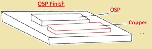
OSP is a thin organic coating applied to copper pads to prevent oxidation before soldering. While OSP offers advantages like fine-pitch compatibility and low cost, it is sensitive to environmental factors and handling conditions. Common soldering defects associated with OSP include:
- Poor solder wetting
- Non-wetting or de-wetting
- Weak solder joint strength
- Oxidation-induced solderability degradation
This paper investigates the causes of these defects and suggests corrective measures to enhance soldering reliability.
2. Common OSP Soldering Defects and Root Causes
2.1 Poor Solder Wetting
Symptoms:
- Solder does not spread evenly on the pad.
- Incomplete fillet formation.
Root Causes:
- OSP Degradation: OSP coating decomposes if exposed to high humidity or elevated temperatures before soldering.
- Excessive Reflow Temperature: If the reflow profile exceeds OSP’s thermal stability limit (~250°C), the coating may burn off prematurely, leading to copper oxidation.
- Contaminated Surfaces: Fingerprints, oils, or flux residues can hinder solder wetting.
2.2 Non-Wetting/De-Wetting
Symptoms:
- Solder balls up instead of adhering to the pad.
- Exposed copper after soldering.
Root Causes:
- Oxidized Copper: If OSP is damaged or expired, copper oxidizes, preventing proper solder bonding.
- Insufficient Flux Activity: Weak flux cannot remove oxides effectively.
- Improper Reflow Profile: Insufficient peak temperature or dwell time prevents proper IMC formation.
2.3 Weak Solder Joint Strength
Symptoms:
- Brittle or cracked solder joints.
- Poor mechanical reliability.
Root Causes:
- Insufficient IMC Formation: OSP requires proper thermal exposure to allow Cu-Sn intermetallic bonding.
- OSP Residue Interference: Incomplete OSP decomposition may leave organic residues at the joint interface.
2.4 Oxidation-Induced Solderability Degradation
Symptoms:
- Darkened or discolored pads before soldering.
- Increased soldering defects after prolonged storage.
Root Causes:
- Humidity Exposure: OSP-coated PCBs absorb moisture, accelerating copper oxidation.
- Long Storage Time: OSP has a limited shelf life (typically 6–12 months).
3. Improvement Strategies
3.1 Optimizing PCB Storage and Handling
- Controlled Environment: Store OSP PCBs in nitrogen-sealed bags with desiccants (humidity < 40%).
- Limited Shelf Life: Use FIFO (First-In-First-Out) inventory management to avoid expired OSP coatings.
- Avoid Direct Handling: Wear gloves to prevent contamination from skin oils.
3.2 Reflow Profile Optimization
- Preheat Stage: Gradual heating (1–2°C/sec) to prevent OSP blistering.
- Peak Temperature: Maintain 230–245°C to ensure OSP decomposition without burning.
- Time Above Liquidus (TAL): 60–90 sec to allow proper IMC formation.
3.3 Flux Selection and Application
- High-Activity Flux: Use no-clean or mildly activated rosin-based flux for better oxide removal.
- Adequate Flux Coverage: Ensure sufficient flux application to prevent oxidation during reflow.
3.4 Rework and Secondary Reflow Considerations
- Nitrogen Reflow: Use nitrogen-assisted reflow to minimize oxidation during rework.
- Localized Heating: Avoid excessive heat exposure to adjacent components.
3.5 Alternative Surface Finishes for Critical Applications
If OSP-related defects persist, consider alternative finishes:
- ENIG (Electroless Nickel Immersion Gold): Better oxidation resistance but higher cost.
- Immersion Silver (IAg): Good solderability but prone to tarnishing.
- HASL (Hot Air Solder Leveling): Robust but not suitable for fine-pitch components.

4. Case Study: OSP Soldering Defect Resolution
A manufacturing facility observed a 15% defect rate in OSP-coated PCBs during reflow. Analysis revealed:
- Root Cause: Improper storage (high humidity) and aggressive reflow profile.
- Solution:
- Implemented dry storage with humidity indicators.
- Adjusted reflow profile to a gentler ramp-up and optimized peak temperature.
- Result: Defect rate reduced to <2%.
5. Conclusion
OSP surface treatment is cost-effective but requires careful handling and process control to prevent soldering defects. Key improvements include:
- Proper storage and handling to prevent OSP degradation.
- Optimized reflow profiles for complete OSP decomposition.
- High-activity flux to enhance wetting.
- Nitrogen-assisted reflow for rework processes.
By implementing these strategies, manufacturers can significantly reduce OSP-related soldering defects and improve PCB assembly reliability.