Panasonic Megtron 6 Datasheet: HDI and Thermal Performance

Key Takeaways
Panasonic Megtron 6 sets a benchmark in PCB manufacturing for high-frequency applications, combining ultra-low dielectric loss with advanced thermal stability. If you’re designing 5G infrastructure or high-speed networking hardware, this material’s low Dk/Df glass cloth minimizes signal attenuation, enabling cleaner data transmission even in multilayer HDI layouts. For PCB manufacturing companies, the optimized thermal conductivity (0.5 W/m·K) ensures reliable heat dissipation, reducing hotspots in densely packed circuits—a critical factor for mission-critical systems.
“When selecting materials for high-frequency PCB designs, prioritize dielectric properties and thermal stability to ensure signal integrity across operating temperatures.”
The H-VLP copper foil specification enhances signal integrity by reducing surface roughness to ≤1.5 µm, which is particularly advantageous for designs requiring impedance control below 28 GHz. When comparing Megtron 6 to standard FR-4 or mid-loss laminates, you’ll notice a 40% reduction in insertion loss at 10 GHz—translating to longer signal reach in data centers. For businesses evaluating PCB manufacturing cost, Megtron 6’s durability reduces rework risks, balancing upfront material expenses with long-term reliability.
With 5G’s rollout demanding tighter tolerances, this material’s ultra-low loss characteristics (Df ≤0.0015 at 10 GHz) make it a strategic choice for antenna modules and beamforming circuits. For stakeholders in the PCB manufacturing business, accessing the full datasheet provides critical insights into layer stack-up recommendations and processing guidelines, ensuring optimal performance without compromising yield rates.
Panasonic Megtron 6 PCB Material Overview
When selecting materials for advanced PCB manufacturing, engineers prioritize substrates that balance electrical performance, thermal stability, and cost efficiency. Panasonic’s Megtron 6 emerges as a standout choice for high-frequency applications, offering a unique combination of ultra-low dissipation factor (Df) and controlled dielectric constant (Dk). Designed to meet the demands of 5G infrastructure and high-speed networking equipment, this material leverages specialized low Dk glass cloth to minimize signal loss while maintaining consistent impedance control—a critical factor for PCB manufacturing companies aiming to reduce post-production tuning.
The material’s thermal management capabilities stem from its optimized resin system, which ensures stable performance even under elevated temperatures. For businesses analyzing PCB manufacturing cost, Megtron 6’s ability to support thinner multilayer designs reduces layer counts and simplifies fabrication processes. This translates to lower material waste and faster assembly cycles, particularly beneficial for high-mix, low-volume production runs common in the PCB manufacturing business.
A key innovation lies in its H-VLP (Hyper Very Low Profile) copper foil, which enhances signal integrity by minimizing surface roughness. This feature becomes particularly crucial when designing high-density interconnects (HDIs) for millimeter-wave applications. By integrating Megtron 6 into your stackup, you gain access to a substrate that aligns with industry standards like IPC-4103 while outperforming traditional FR-4 alternatives in insertion loss and thermal reliability.
For detailed specifications, including glass transition temperature (Tg) ranges and copper peel strength metrics, refer to Panasonic’s material selection guide. Whether optimizing for PCB manufacturing cost or pushing the limits of signal speed, Megtron 6 provides a scalable solution that adapts to evolving technical requirements without compromising manufacturability.

HDI Performance in High-Speed Networks
When designing high-density interconnect (HDI) circuits for 5G infrastructure or high-speed networking equipment, the choice of substrate material directly impacts signal integrity and thermal stability. Panasonic Megtron 6 addresses these challenges through its ultra-low dielectric loss and advanced HDI-compatible architecture, making it a preferred choice for PCB manufacturing companies aiming to balance performance and PCB manufacturing cost.
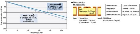
The material’s low Dk glass cloth (Dk = 3.7 at 10 GHz) minimizes signal distortion in tightly packed multilayer designs, which is critical for maintaining impedance control in high-frequency applications. For PCB manufacturing businesses handling complex layouts, this translates to reduced crosstalk and improved signal propagation speeds—key factors for 28+ Gbps data rates in modern routers and switches.
| Property | Megtron 6 | Standard FR-4 |
|---|---|---|
| Dielectric Constant (Dk) | 3.7 @ 10 GHz | 4.5 @ 10 GHz |
| Dissipation Factor (Df) | 0.0015 | 0.020 |
| Thermal Conductivity (W/m·K) | 0.75 | 0.25 |
This table highlights why PCB manufacturing workflows leveraging Megtron 6 achieve better thermal dissipation and lower insertion loss compared to conventional materials. The H-VLP copper foil further enhances signal integrity by reducing surface roughness, which is vital for minimizing skin effect losses in millimeter-wave frequencies.
For PCB manufacturing cost optimization, the material’s compatibility with laser drilling and sequential lamination processes reduces post-processing steps. You can achieve finer traces (≤ 25 μm) and microvias without compromising reliability, even in high-temperature environments. This makes it easier to meet the stringent tolerances required for 5G antenna modules or data center backplanes, while keeping production timelines predictable.
By integrating Megtron 6 into your designs, you’re not just selecting a substrate—you’re adopting a solution that aligns with the thermal and electrical demands of next-gen networks. Its performance in HDI applications ensures that signal paths remain efficient, even as component densities continue to rise.
Thermal Management Capabilities Explained
When designing high-frequency circuits for 5G applications or high-speed networking equipment, managing heat dissipation becomes a critical factor in maintaining system reliability. Panasonic’s Megtron 6 addresses this challenge through its advanced thermal conductivity (0.8 W/m·K) and a low coefficient of thermal expansion (CTE) of 3 ppm/°C, which minimizes dimensional shifts under extreme operating temperatures. For PCB manufacturing companies, this translates to stable signal integrity even in environments where components generate significant heat, such as power amplifiers or server-grade hardware.
The material’s glass transition temperature (Tg) of 180°C ensures structural stability during both PCB manufacturing processes and end-use scenarios. This is particularly valuable when addressing PCB manufacturing cost considerations, as higher Tg materials reduce risks of warping or delamination during reflow soldering—common pain points in multilayer HDI designs. By maintaining consistent performance across thermal cycles, Megtron 6 helps PCB manufacturing businesses avoid costly rework or field failures.
Another standout feature is its balanced thermal dissipation rate, which prevents localized hotspots in dense circuit layouts. This capability is essential for high-power RF modules or data center switches, where uneven heat distribution can degrade adjacent components. Engineers working with high-speed designs will appreciate how Megtron 6’s thermal properties complement its low Dk glass cloth, enabling tighter impedance control without sacrificing heat management.
For applications demanding prolonged operational lifespans—such as automotive radar or telecom infrastructure—the material’s resistance to thermal aging ensures minimal degradation over time. This reliability directly impacts PCB manufacturing cost efficiency by extending maintenance intervals and reducing warranty claims.
By integrating Megtron 6 into your stack-up, you gain a material engineered to harmonize thermal resilience with electrical performance—a balance that’s non-negotiable in next-generation PCB manufacturing.
Low Dk Glass Cloth Technical Specifications
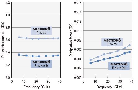
When selecting materials for high-frequency applications, the dielectric constant (Dk) of glass cloth becomes a critical factor in minimizing signal loss. Panasonic Megtron 6 employs a specialized low Dk glass cloth engineered to maintain consistent performance across a broad frequency range, making it ideal for 5G infrastructure and high-speed networking equipment. With a Dk value of 3.7 at 10 GHz, this material reduces capacitive coupling between traces, enabling tighter impedance control—a necessity for advanced PCB manufacturing processes requiring high-density interconnects (HDI).
For PCB manufacturing companies, the glass cloth’s thermal stability is equally vital. Megtron 6’s composition ensures minimal Dk variation (±0.05) even under temperature fluctuations up to 180°C, which directly impacts PCB manufacturing cost by reducing rework rates during thermal cycling tests. This consistency also simplifies design validation, as engineers can rely on predictable signal integrity across operating conditions.
The material’s low dissipation factor (Df), typically 0.0015 at 10 GHz, further enhances its suitability for millimeter-wave applications. By minimizing energy absorption, it allows PCB manufacturing businesses to meet stringent insertion loss requirements for 28 GHz+ 5G antenna modules. Additionally, the glass cloth’s smooth surface profile improves adhesion with H-VLP copper foil, reducing micro-void formation during lamination—a common pain point in high-layer-count boards.
While optimizing for performance, Megtron 6 maintains compatibility with standard PCB manufacturing workflows. Its glass transition temperature (Tg) of 180°C ensures dimensional stability during lead-free soldering, avoiding delamination risks that could escalate production costs. For designers balancing signal integrity and manufacturability, these technical specifications create a robust foundation for next-generation RF and high-speed digital designs.
H-VLP Copper Foil for Signal Integrity
When designing high-speed circuits, maintaining signal integrity becomes critical—especially in applications like 5G infrastructure or data centers. Panasonic’s Megtron 6 addresses this challenge with its H-VLP (Hyper Very Low Profile) copper foil, engineered to minimize insertion loss and impedance fluctuations. Unlike standard rolled copper, H-VLP copper foil features a smoother surface roughness (typically ≤ 0.3 µm), reducing skin effect losses at frequencies above 10 GHz. This makes it indispensable for PCB manufacturing workflows where high-frequency performance cannot be compromised.
For PCB manufacturing companies, integrating H-VLP copper into multilayer designs requires precise process controls. The foil’s ultra-thin profile (as low as 2 µm) demands specialized etching techniques to avoid over- or under-etching, which could degrade impedance matching. However, the trade-off is clear: boards built with this material exhibit up to 20% lower signal attenuation compared to conventional options, directly impacting system reliability in dense, high-speed layouts.
Balancing PCB manufacturing cost and performance is a recurring dilemma. While H-VLP copper adds a premium to raw material expenses, its ability to reduce post-production tuning and minimize signal retries offsets long-term operational costs. For instance, in a 24-layer server motherboard, using Megtron 6 with H-VLP foil can cut signal integrity validation cycles by 30–40%, accelerating time-to-market for PCB manufacturing business clients.
The thermal stability of H-VLP copper further complements Megtron 6’s low Dk glass cloth, ensuring consistent performance under thermal stress. This synergy is vital for applications like automotive radar or AI accelerators, where temperature swings can destabilize high-frequency signals. By prioritizing both electrical and mechanical precision, Panasonic’s solution enables engineers to push the boundaries of high-density interconnect (HDI) designs without sacrificing signal clarity.
Transitioning to H-VLP copper isn’t just about material choice—it’s a strategic upgrade for PCB manufacturing workflows aiming to meet next-gen connectivity standards. Whether optimizing for millimeter-wave 5G or 400G Ethernet, this foil ensures your designs stay ahead of bandwidth demands while maintaining manufacturability at scale.
5G Applications and Ultra-Low Loss Benefits
As 5G networks demand faster data transmission and reduced latency, PCB manufacturing faces unprecedented challenges in balancing signal integrity with thermal efficiency. Panasonic Megtron 6 addresses these needs by offering ultra-low dissipation factors (Df) below 0.0015 at 10 GHz, minimizing signal attenuation in high-frequency environments. For PCB manufacturing companies, this translates to improved performance in millimeter-wave applications—critical for 5G base stations, small-cell antennas, and edge computing infrastructure.
The material’s low dielectric constant (Dk) of 3.2–3.4 across a wide frequency range ensures stable impedance control, reducing design complexity for multi-layer HDI boards. When optimizing PCB manufacturing cost, Megtron 6’s thermal conductivity (0.6 W/m·K) becomes a key advantage. It dissipates heat more effectively than standard FR-4 materials, lowering the risk of thermal stress in densely packed 5G components. This thermal resilience directly impacts long-term reliability, a critical factor for network operators managing 24/7 uptime requirements.
For businesses scaling their PCB manufacturing business in 5G markets, Megtron 6’s compatibility with H-VLP (Hyper Very Low Profile) copper foil further enhances signal integrity. The ultra-smooth copper surface reduces skin effect losses at high frequencies, maintaining clean signal transitions even in complex RF designs. This combination of low loss and thermal stability enables thinner trace geometries without sacrificing performance—ideal for miniaturized 5G devices requiring strict space constraints.
While evaluating materials, engineers should note that Megtron 6’s ultra-low loss properties align with 3GPP Release 16 specifications for 5G NR (New Radio). This compliance ensures seamless integration into existing PCB manufacturing workflows while future-proofing designs for emerging technologies like 6G research prototypes. By minimizing retooling needs and material waste, the substrate helps balance upfront PCB manufacturing cost with lifecycle value—a strategic consideration in capital-intensive 5G deployments.
Comparing Megtron 6 to Industry Standards
When evaluating materials for PCB manufacturing, you’ll find that Panasonic’s Megtron 6 stands apart from conventional substrates in critical performance metrics. Unlike standard FR-4 or even many high-speed laminates, Megtron 6 achieves a dielectric constant (Dk) of 2.3–2.8 at 10 GHz, significantly lower than the 3.5–4.5 range typical of mid-tier materials. This ultra-low Dk directly translates to reduced signal loss, a non-negotiable requirement for 5G infrastructure and high-frequency applications. For PCB manufacturing companies, this means fewer compromises between signal integrity and layer count in HDI designs.
Thermally, Megtron 6’s glass transition temperature (Tg) of 180°C and thermal conductivity of 0.6 W/m·K outperform most industry alternatives, which often plateau at 150°C Tg and 0.4 W/m·K. These properties enable better heat dissipation in dense layouts, lowering the risk of delamination during reflow cycles—a critical factor when calculating PCB manufacturing cost for high-reliability systems. While some specialty materials claim similar thermal stability, they often sacrifice processability or require exotic fabrication techniques that inflate production timelines.
The material’s H-VLP copper foil further differentiates it, offering surface roughness below 1.5 μm compared to the 2–3 μm range seen in standard rolled copper. Smoother copper surfaces minimize skin effect losses at millimeter-wave frequencies, allowing your PCB manufacturing business to meet stringent insertion loss budgets without over-engineering stackups. When benchmarked against competing high-speed substrates like Isola’s Astra MT77 or Rogers’ RO4000 series, Megtron 6 delivers comparable electrical performance but with superior moisture resistance and z-axis CTE control—attributes that reduce warpage risks in multilayer assemblies.
By aligning Megtron 6’s datasheet specifications with real-world PCB manufacturing requirements, you gain a substrate that bridges the gap between cutting-edge performance and manufacturable scalability. Its balanced profile makes it particularly viable for applications where both thermal management and signal fidelity dictate material selection.
Download Full Datasheet and Design Guide
When working with advanced materials like Panasonic Megtron 6, accessing the complete datasheet and design guide is critical for optimizing your PCB manufacturing workflow. These documents provide granular insights into material properties, including low Dk glass cloth specifications and H-VLP copper foil tolerances, which directly influence signal integrity in high-frequency applications. For PCB manufacturing companies, understanding these parameters ensures precise layer stackup design and minimizes impedance mismatches—key factors in reducing PCB manufacturing cost while maintaining performance.
The design guide complements the datasheet by offering application-specific recommendations, such as thermal management strategies for 5G infrastructure or HDI layout rules for dense interconnects. This becomes particularly valuable when balancing performance targets with PCB manufacturing business constraints, such as material yield and production scalability. For instance, the guide details optimal lamination cycles for Megtron 6’s ultra-low-loss dielectric, helping you avoid delamination risks during multilayer assembly.
By integrating the datasheet’s electrical performance data (like Df and Dk values across frequencies) with the design guide’s best practices, you can streamline prototyping and avoid costly revisions. The resources also include comparative charts against industry standards like Isola FR408HR or Rogers materials, empowering informed material substitutions without compromising thermal or signal integrity requirements.
To download these essential documents, visit Panasonic’s official portal or authorized distributor platforms. Ensure your team cross-references the latest revisions, as updates often reflect new findings on Megtron 6’s compatibility with emerging PCB manufacturing techniques like mSAP (modified semi-additive process) or hybrid laser drilling. Equipping your engineers with these resources not only accelerates design cycles but also strengthens your PCB manufacturing business’s ability to tackle next-gen networking and automotive projects.
Conclusion
When selecting materials for advanced pcb manufacturing, the choice of substrate directly impacts both performance and pcb manufacturing cost. Panasonic Megtron 6 exemplifies how cutting-edge materials can address the dual challenges of high-density interconnect (HDI) design and thermal management in modern electronics. For pcb manufacturing companies, leveraging its ultra-low loss characteristics ensures signal integrity in 5G infrastructure and high-speed networks, while its low Dk glass cloth minimizes signal distortion—a critical factor for high-frequency applications.
The material’s H-VLP copper foil further enhances reliability, reducing insertion loss even in complex multilayer designs. This becomes particularly evident when balancing pcb manufacturing business priorities, where long-term reliability often outweighs upfront material costs. Engineers working on thermally demanding applications will appreciate Megtron 6’s optimized heat dissipation, which simplifies thermal management strategies without compromising board density.
It’s worth noting that while Megtron 6 may initially appear costlier than conventional materials, its performance advantages often justify the investment—especially for projects requiring strict impedance control or extended operational lifespans. For businesses focused on pcb manufacturing for mission-critical systems, integrating this substrate can streamline production workflows and reduce post-deployment failures.
Ultimately, the datasheet serves as a blueprint for optimizing both design and manufacturing processes. By aligning material properties with application requirements, you ensure that every layer of your PCB contributes to a robust, future-proof solution.
Frequently Asked Questions
How does Megtron 6 impact PCB manufacturing costs for high-frequency applications?
While PCB manufacturing companies may initially face higher material costs compared to standard FR-4, Megtron 6’s ultra-low loss properties reduce signal attenuation in 5G systems. This minimizes the need for additional signal-boosting components, offsetting upfront expenses over the product lifecycle.
What makes Megtron 6 suitable for HDI designs in dense PCB layouts?
The material’s low Dk/Df characteristics enable tighter trace spacing without cross-talk risks, allowing PCB manufacturing businesses to achieve higher layer counts in compact form factors. Its compatibility with laser drilling supports microvia creation for advanced HDI architectures.
Can this material withstand thermal stresses in automotive PCB manufacturing?
Yes, Megtron 6’s thermal decomposition temperature (Td) of 340°C exceeds industry benchmarks, ensuring reliability during reflow soldering and high-temperature operation. This makes it ideal for ADAS systems and engine control units where thermal cycling is frequent.
How do H-VLP copper foils improve performance in high-speed networks?
The ultra-smooth H-VLP copper surface reduces skin effect losses at millimeter-wave frequencies, critical for 28GHz+ 5G deployments. PCB manufacturing teams leverage this to maintain impedance consistency across multi-gigabit channels.
What design tools support Megtron 6 integration for new PCB manufacturing projects?
Panasonic provides 3D electromagnetic simulation models compatible with Altium and Cadence platforms. These accelerate material-specific optimizations for insertion loss and heat dissipation, reducing prototyping iterations.
Ready to Optimize Your Next PCB Design?
For tailored solutions using Panasonic Megtron 6 in your PCB manufacturing workflow, please click here to consult our signal integrity experts and request material samples.