Parameters Involved in PCB Layout
When you are not used to a new set of PCB design tools, the large number of parameters that need to be set can be overwhelming. But you have to get familiar with it because, through its proper handling of controls, the layout tool can be made to fit your design methods and style. Here are the issues about PCB layout parameters and how to use them to adjust the design environment for maximum productivity.
Why do you need all these parameters in the design tool for PCB layout?
Since the first introduction of PCB design tools, layout engineers have been looking for more and more features. Design tools 40 years ago would allow you to move parts and draw tracks, but there was little else. Footprint changes of individual components were difficult to operate, area fill (copper pour) functions were primitive at best, and there were many other restrictions on how you could work due to the limitations of the tools. Over time, these limitations were eliminated with the advancement of hardware and software. However, these advances brought a new set of problems that must be solved. All of these new features require more and more setup time to function properly.
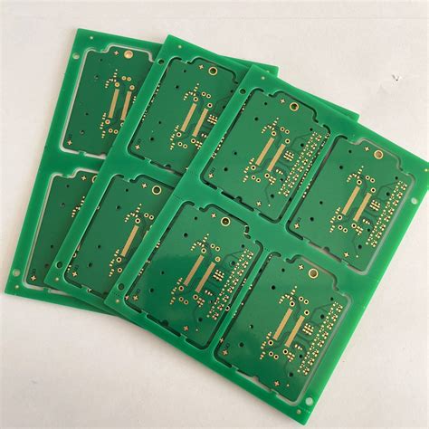
As the number of layers increases, it becomes more difficult to visually identify each design element on the screen, and existing grid and rule structures cannot control it as new routing and area fill capabilities are added. These are just a few of the important issues that need to be addressed as the design capabilities of the tools are increased. If you have ever worked on a 16-layer board using a design system from 35 years ago, the system only provided a monochrome display. Without the ability to set different colors, it would be almost impossible to use.
In order to give users more flexibility in using the new enhancements in PCB design CAD systems, EDA vendors are beginning to include more and more parameters that need to be set for layout. These parameter settings can be a bit overwhelming when using a new set of design tools, but parameter settings exist for a reason, even if not every user needs to use them:
- Units of measurement, tolerances, fonts, text size, and other standards vary depending on the user’s habits.
- Some people see different colors and patterns than others, and it is necessary to be able to change the display as needed.
- A display scheme may look good for some tasks, such as library development, but it may be distracting or difficult to see when laying out.
- Parameters that benefit one user, such as grid settings, may be difficult for other users to use for the same task.
- Display schemes used by a single user may be difficult for a team to use during a design review.
Of course, there are many other reasons to change the parameters of a CAD system, these are just a few examples. Next, let’s look at some of the parameters that PCB designers would most like to be able to change.
CAD Parameters Most Beneficial to Change
Setting up a PCB design system for the most productive work environment means being able to change the parameters of the tool as needed. Here are some of the parameters that designers would most like to use:
How the design is displayed
lToolbars and Commands: Being able to reposition toolbars, and the commands within them, is one of the top items on the list for making design tools easier to use. While this does not affect the design itself, it does help increase user productivity when users can organize their favorite commands and workflows.
Color: The ability to change colors has long been a user-configurable parameter, but users have been seeking more control over the depth of these selections. Designers want to set color selections not only for layers, but also by net, group, or design object. This can be very useful when working with multiple power and ground nets that must be kept separate.
Patterns and Fills: In addition to color, this is another designer request that goes beyond simple pattern settings. With the ability to change fill patterns or adjust layer shading, specific areas of the design can stand out more than ever before.
How to Use the Tool
Task Settings: PCB layout is characterized by certain tasks, such as footprint creation, component placement, and trace routing. Many of these tasks require specific parameters to be set in order to use the full capabilities of the tool. For example, trace routing can have many different manual and automatic functions to give designers more options. While these tasks have traditionally all required parameter settings, the number of parameters continues to grow with each new enhancement added to the tool. Designers are asking for these parameters to be organized into an easily accessible menu.
Function Settings: Similarly, functions require more parameters. These will include setting up design reports, manufacturing files, and test points, all of which need to be easily accessible and easy to use.
Design Specific Settings
l Units, Grids, and Text: These have been standard parameters available for a long time, but as the complexity of the tools has continued to increase, the number of these settings has also increased. PCB designers have long asked for these settings to be easy to find, use, and be able to read from templates or other sources.
Thankfully, EDA vendors are responding to these user requests, and most design tools are becoming easier to use when setting layout parameters.