PCB 3D Modeling: Techniques, Tools, and Applications
Introduction
Printed Circuit Board (PCB) design has evolved significantly over the years, transitioning from simple 2D layouts to complex 3D models that enhance design accuracy, manufacturability, and performance. 3D modeling of PCBs plays a crucial role in modern electronics design, enabling engineers to visualize, simulate, and optimize their designs before fabrication.
This article explores the fundamentals of PCB 3D modeling, its benefits, key techniques, popular software tools, and real-world applications. By the end, readers will have a comprehensive understanding of how 3D modeling enhances PCB design and manufacturing processes.
1. What is PCB 3D Modeling?
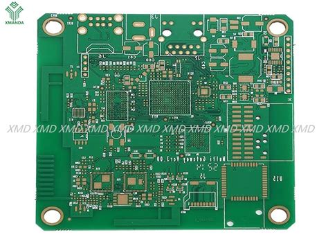
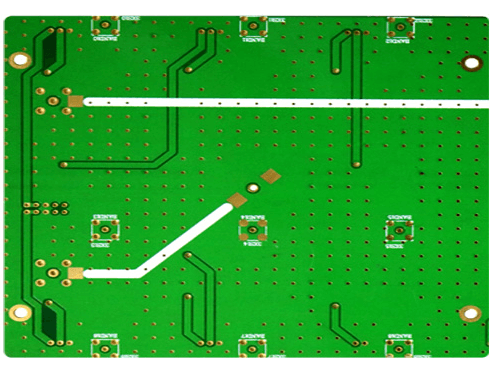
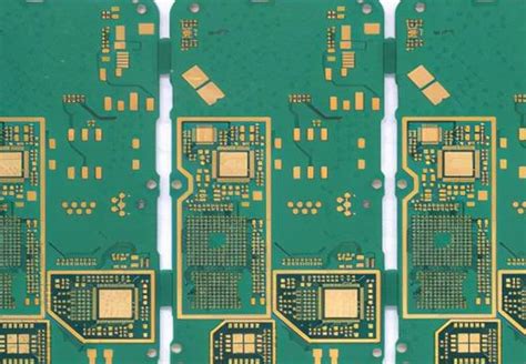
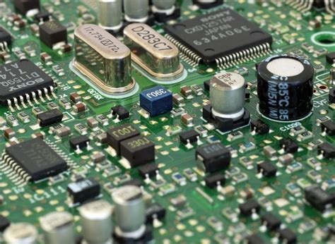
PCB 3D modeling refers to the process of creating a three-dimensional digital representation of a printed circuit board, including its components, traces, vias, and mechanical enclosures. Unlike traditional 2D layouts, 3D models provide a more realistic view of how the PCB will look and function in its final form.
Key Elements of PCB 3D Models:
- Substrate & Layers: The base material (e.g., FR4) and copper layers.
- Components: 3D models of resistors, capacitors, ICs, connectors, etc.
- Traces & Vias: Conductive pathways and inter-layer connections.
- Mechanical Enclosures: Housing, heatsinks, and mounting points.
2. Benefits of PCB 3D Modeling
2.1 Enhanced Design Accuracy
- Detects component collisions and placement errors early.
- Ensures proper clearances between parts and enclosures.
- Improves thermal management by visualizing heat dissipation.
2.2 Improved Manufacturing Efficiency
- Reduces prototyping costs by identifying issues before production.
- Facilitates Design for Manufacturability (DFM) checks.
- Helps in automated assembly by validating pick-and-place paths.
2.3 Better Collaboration & Visualization
- Allows engineers, manufacturers, and clients to interact with a realistic model.
- Supports virtual prototyping for faster design iterations.
- Enables augmented reality (AR) and virtual reality (VR) reviews.
2.4 Electromagnetic & Thermal Simulation
- Signal Integrity (SI) Analysis: Identifies EMI/EMC issues.
- Thermal Analysis: Predicts hotspots and optimizes cooling solutions.
- Mechanical Stress Testing: Ensures durability under vibration or shock.
3. Key Techniques in PCB 3D Modeling
3.1 Component Library Integration
- STEP Models: Standardized 3D models (ISO 10303) for components.
- ECAD-MCAD Collaboration: Synchronization between electrical and mechanical CAD tools.
3.2 Realistic Material Properties
- Dielectric Constants: Simulating signal behavior in different substrates.
- Thermal Conductivity: Analyzing heat flow in copper and PCB materials.
- Flex & Rigid-Flex Modeling: Simulating bendable PCBs.
3.3 Automated Design Rule Checks (DRC)
- Clearance Verification: Ensures no short circuits in 3D space.
- Height Restrictions: Confirms components fit within enclosures.
- Assembly Feasibility: Validates solder paste and stencil alignment.
3.4 Exporting for Simulation & Prototyping
- Finite Element Analysis (FEA): Structural and thermal simulations.
- 3D Printing: Rapid prototyping of PCB enclosures.
- Augmented Reality (AR) Overlays: Real-world PCB visualization.
4. Popular PCB 3D Modeling Software Tools
4.1 Altium Designer
- Features: Integrated ECAD/MCAD, real-time 3D clearance checks.
- Advantages: High compatibility with mechanical CAD tools like SolidWorks.
4.2 KiCad
- Features: Free & open-source, supports STEP model imports.
- Advantages: Growing library of 3D components.
4.3 Autodesk Eagle
- Features: Fusion 360 integration for mechanical modeling.
- Advantages: Cloud-based collaboration.
4.4 Cadence Allegro
- Features: Advanced SI/PI and thermal analysis.
- Advantages: High-speed PCB design optimization.
4.5 Siemens Xpedition
- Features: Rigid-flex PCB modeling, DFM validation.
- Advantages: Enterprise-level PCB design.
5. Applications of PCB 3D Modeling
5.1 Consumer Electronics
- Smartphones, wearables, and IoT devices benefit from miniaturization and thermal optimization.
5.2 Automotive & Aerospace
- High-reliability PCBs for ADAS (Advanced Driver Assistance Systems) and avionics.
5.3 Medical Devices
- Implantable electronics and diagnostic equipment require precise 3D modeling.
5.4 Industrial Automation
- Robotics & motor control PCBs need mechanical and thermal validation.
5.5 Flexible & Wearable Electronics
- Bendable PCBs for foldable displays and flexible sensors.
6. Future Trends in PCB 3D Modeling
6.1 AI-Driven Design Optimization
- Machine learning algorithms for auto-routing and thermal management.
6.2 Advanced Multi-Board Simulations
- Modeling entire systems (PCBs, cables, enclosures) in a unified 3D environment.
6.3 Cloud-Based Collaboration
- Real-time multi-user editing and version control.
6.4 Integration with Additive Manufacturing
- 3D-printed electronics combining conductive inks with traditional PCBs.
6.5 Virtual & Augmented Reality (VR/AR)
- Immersive PCB reviews for design validation.
Conclusion
PCB 3D modeling is revolutionizing electronics design by bridging the gap between electrical and mechanical engineering. With advanced simulation capabilities, better visualization, and seamless integration with manufacturing processes, 3D modeling ensures higher reliability, reduced costs, and faster time-to-market.
As technology evolves, the adoption of AI, cloud computing, and AR/VR will further enhance PCB design workflows, making 3D modeling an indispensable tool for modern electronics engineers.