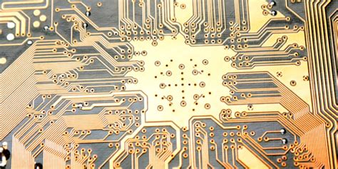
PCB and integrated circuits
Current circuit boards are mainly composed of the following:
- Circuits and patterns: Circuits are used as a tool for conducting between components. In the design, a large copper surface will be designed as the ground and power supply layer. Circuits and patterns are made at the same time.
- Dielectric layer: Used to maintain the insulation between circuits and layers, commonly known as substrate.
- Through hole (via): Through holes can make circuits above two levels conduct to each other. Larger through holes are used for component plug-ins. In addition, non-through holes (nPTH) are usually used for surface mounting positioning and fixing screws during assembly. China IC Network
- Solder resistant ink (Solder resistant /Solder Mask): Not all copper surfaces need to be tinned with components. Therefore, a layer of material (usually epoxy resin) will be printed in the non-tinned areas to prevent the copper surface from tinning and avoid short circuits between non-tinned circuits. According to different processes, it is divided into green oil, red oil, and blue oil.
- Silk screen (Legend /Marking/Silk screen): This is a non-essential component. Its main function is to mark the names and position frames of each part on the circuit board for easy maintenance and identification after assembly. ‘ ]: R4 d, k: p6 v, D! L9 P8 c
- Surface treatment (Surface Finish): Since the copper surface is easily oxidized in the general environment, it cannot be tinned (poor solderability), so it will be protected on the copper surface that needs to be tinned. The protection methods include HASL, ENIG, Immersion Silver, Immersion TIn, and Organic Solder Preservative (OSP). Each method has its own advantages and disadvantages, and is collectively referred to as surface treatment.
PCB board features2 ^’ | W; k4 I2 I6 }/ a5 r* n - High density: For decades, the high density of printed circuit boards has been developing with the improvement of integrated circuit integration and the advancement of installation technology. * G8 E’ ~’ m( F# V
- High reliability: Through a series of inspections, tests and aging tests, the PCB can be guaranteed to work reliably for a long time (usage period, generally 20 years).
- Designability: For various performance requirements of PCB (electrical, physical, chemical, mechanical, etc.), the printed board design can be realized through design standardization and normalization, which is short in time and high in efficiency.
- Producibility: With modern management, standardized, scaled (quantified), automated production can be carried out to ensure product quality consistency.( R- t7 F* k6 n’ x, E, |
- Testability: A relatively complete test method, test standard, various test equipment and instruments have been established to detect and identify the qualification and service life of PCB products.
Assemblyability: PCB products are convenient for standardized assembly of various components, and can also be automated and mass-produced. At the same time, PCB and various component assembly parts can also be assembled into larger components, systems, and even complete machines. - Maintainability: Since PCB products and various component assembly parts are designed and mass-produced in a standardized manner, these parts are also standardized. Therefore, once a system fails, it can be replaced quickly, conveniently and flexibly to quickly restore the system to work. Of course, more examples can be given. For example, making the system miniaturized and lightweight, and speeding up signal transmission.
Features of integrated circuits” ]! q’ L$ O% h3 D d. q/ ?
Integrated circuits have the advantages of small size, light weight, fewer lead wires and welding points, long life, high reliability, good performance, etc., and low cost, which is convenient for large-scale production. It is not only widely used in industrial and civilian electronic equipment such as recorders, televisions, computers, etc., but also in military, communications, remote control, etc. Using integrated circuits to assemble electronic equipment, its assembly density can be increased by dozens to thousands of times compared with transistors, and the stable working time of the equipment can also be greatly improved.7 Y% Y: x; L4 u5 ! p# v
Application examples of integrated circuits
1.555 touch timing switch
IC1 is a 555 timing circuit, which is connected here as a monostable circuit. Usually, since there is no induced voltage at the touch piece P end, the capacitor C1 is discharged through the 7th foot of 555, the output of the 3rd foot is low level, the relay KS is released, and the light is off. China IC Network, q- {$ \7 H, [( `8 w$ C
When you need to turn on the light, touch the metal sheet P with your hand, and the voltage of the clutter signal induced by the human body is added to the trigger end of 555 from C2, so that the output of 555 changes from low to high level, the relay KS is attracted, and the light is on. At the same time, the 7th foot of 555 is cut off internally, and the power supply charges C1 through R1, which is the beginning of the timing.
When the voltage on the capacitor C1 rises to 2/3 of the power supply voltage, the 7th foot of 555 is turned on to discharge C1, so that the output of the 3rd foot changes from high level back to low level, the relay is released, the light goes out, and the timing ends.
The timing length is determined by R1 and C1: T1=1.1R1*C1. According to the value marked in the figure, the timing time is about 4 minutes. D1 can choose 1N4148 or 1N4001. * i) r3 j- e5 m6 `* g
2.Single power supply to dual power supply circuit
In the attached circuit, the time base circuit 555 is connected as an astable circuit, and the 3-pin output frequency is 20KHz and the duty cycle is 1:1 square wave. When the 3-pin is high level, C4 is charged; when the 3-pin is low level, C3 is charged. Due to the existence of VD1 and VD2, C3 and C4 are only charged but not discharged in the circuit, and the maximum charging value is EC. When the B end is grounded, the +/-EC dual power supply is obtained at the A and C ends. The output current of this circuit exceeds 50mA. 8 P( x0 n/ G, T; K* ]! J
Differences between PCB and integrated circuits/ L7 T’ M* I I2 O3 x# e
Integrated circuits generally refer to the integration of chips, such as the north bridge chip on the motherboard and the inside of the CPU, which are all called integrated circuits. The original name is also called integrated circuits. Printed circuits refer to the circuit boards we usually see, and there are also printed and soldered chips on the circuit boards


