PCB Antennas and Electromagnetic Compatibility (EMC): Design, Challenges, and Solutions
Abstract
Printed Circuit Board (PCB) antennas are widely used in modern wireless communication systems due to their compact size, low cost, and ease of integration. However, their design and implementation must consider Electromagnetic Compatibility (EMC) to ensure reliable operation without interfering with other electronic systems. This paper explores the fundamentals of PCB antennas, their interaction with EMC, key design challenges, and mitigation techniques to enhance performance while complying with regulatory standards.
1. Introduction
The increasing demand for wireless connectivity in IoT devices, smartphones, and embedded systems has driven the adoption of PCB antennas. Unlike traditional external antennas, PCB antennas are etched directly onto the circuit board, reducing manufacturing costs and improving form factor. However, integrating antennas into PCBs introduces electromagnetic interference (EMI) risks, making EMC a critical consideration.
This paper discusses:
- The basics of PCB antenna design.
- EMC challenges in PCB antenna integration.
- Techniques to optimize antenna performance while minimizing EMI.
- Compliance with international EMC standards.
2. Fundamentals of PCB Antennas
2.1 Types of PCB Antennas
Common PCB antenna configurations include:
- Microstrip Patch Antennas: Compact and suitable for high-frequency applications.
- Inverted-F Antennas (IFA): Used in mobile devices due to their small footprint.
- Meandered Dipole Antennas: Optimized for size reduction by increasing electrical length.
- Planar Inverted-F Antennas (PIFA): Offer good bandwidth and radiation efficiency.
2.2 Key Design Parameters
- Frequency Band: Determines antenna dimensions (e.g., 2.4 GHz for Wi-Fi, 5 GHz for 5G).
- Impedance Matching: Ensures maximum power transfer (typically 50 Ω).
- Radiation Pattern: Influences signal coverage and directionality.
- Ground Plane Effects: Critical for antenna performance and EMI control.
3. Electromagnetic Compatibility (EMC) Considerations
EMC ensures that electronic devices operate without causing or suffering from EMI. PCB antennas can be both sources and victims of interference, necessitating careful design.
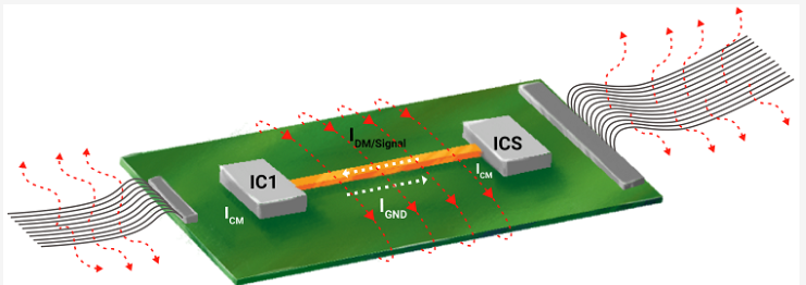
3.1 EMI Sources in PCB Antennas
- Radiated Emissions: High-frequency signals from the antenna may interfere with nearby circuits.
- Conducted Emissions: Noise coupled through power and signal lines.
- Ground Loops: Poor grounding leads to unwanted radiation and susceptibility.
3.2 EMC Challenges
- Crosstalk: Coupling between antenna traces and adjacent high-speed signals.
- Parasitic Effects: Stray capacitance/inductance alters antenna tuning.
- Shielding Limitations: Metallic enclosures can degrade antenna performance.
4. Design Techniques for EMC Optimization
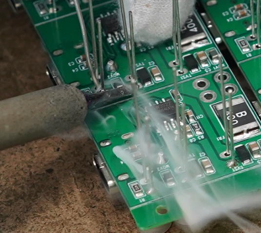
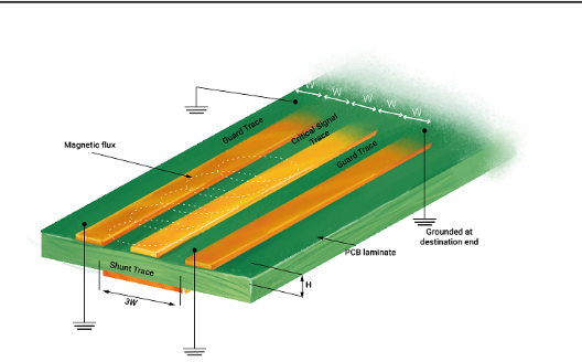
4.1 Proper Grounding Strategies
- Use a continuous ground plane beneath the antenna to minimize loop areas.
- Avoid split grounds that introduce impedance discontinuities.
4.2 Isolation and Shielding
- Keep high-speed digital traces away from the antenna.
- Use shielding cans or ferrite beads to suppress noise.
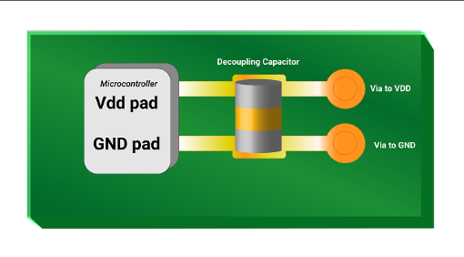
4.3 Filtering and Decoupling
- Implement LC filters on power lines to reduce conducted noise.
- Place decoupling capacitors near RF components.
4.4 Antenna Placement and Layout
- Position the antenna at the board edge to minimize obstruction.
- Avoid placing metal components in the near-field radiation zone.
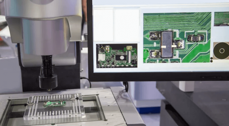
4.5 Simulation and Testing
- Use electromagnetic simulation tools (e.g., HFSS, CST) to predict radiation patterns and EMI.
- Perform pre-compliance EMC testing to identify issues early.
5. Compliance with EMC Standards
Regulatory bodies (FCC, CE, CISPR) impose limits on radiated and conducted emissions. Key standards include:
- FCC Part 15 (USA): Regulates unintentional radiators.
- EN 55032 (EU): CISPR 32 for multimedia equipment emissions.
- IEC 61000-4-3: Immunity to radiated RF fields.
Designers must ensure PCB antennas meet these requirements through proper filtering, shielding, and layout optimization.
6. Case Study: Wi-Fi PCB Antenna Design
A 2.4 GHz Wi-Fi module was designed with a PIFA antenna. Initial testing showed excessive radiated emissions due to poor grounding. By implementing a solid ground plane and adding shielding, emissions were reduced by 12 dB, achieving compliance with FCC Part 15.
7. Future Trends
- 5G and mmWave Antennas: Higher frequencies require advanced EMC techniques.
- Flexible PCBs: New materials impact antenna and EMC performance.
- AI-Driven Optimization: Machine learning for automated EMC-aware antenna design.
8. Conclusion
PCB antennas offer significant advantages in wireless systems but require careful EMC design to prevent interference. By following best practices in grounding, shielding, and layout, engineers can achieve optimal performance while meeting regulatory standards. Future advancements in materials and simulation tools will further enhance EMC-compliant antenna integration.