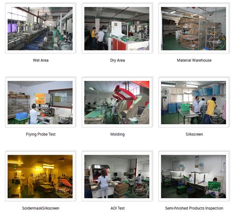
Pcb assembly and testing
Importance Of Solder Paste Inspection In PCB Assembly
In the realm of printed circuit board (PCB) assembly, the importance of solder paste inspection (SPI) cannot be overstated. As the initial step in the surface mount technology (SMT) process, solder paste application sets the foundation for the entire assembly. Any discrepancies at this stage can lead to significant issues down the line, making SPI a critical quality control measure.
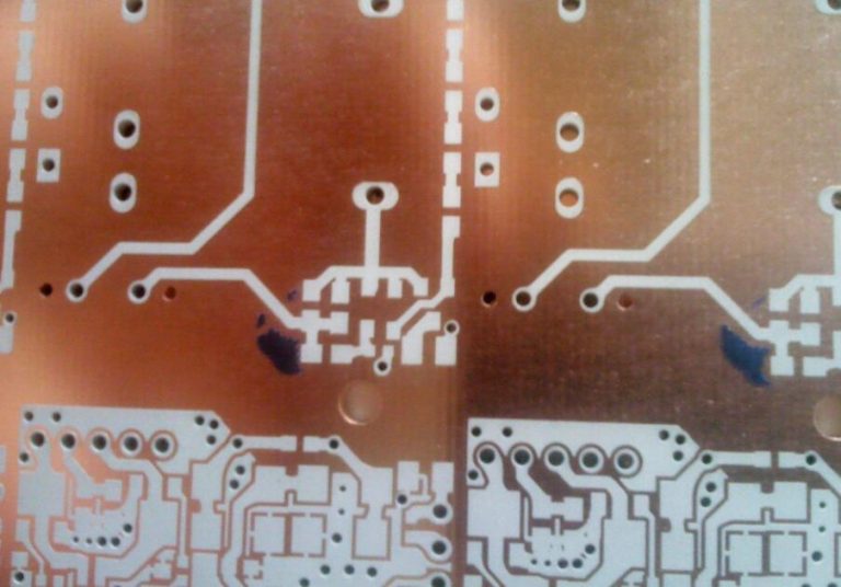
Solder paste, a mixture of powdered solder and flux, is applied to the PCB through a stencil.
This paste serves as the adhesive that holds components in place before reflow soldering. Given its pivotal role, ensuring the correct amount and placement of solder paste is essential. Inaccuracies in solder paste deposition can result in various defects, such as insufficient solder joints, bridging, or tombstoning, which can compromise the functionality and reliability of the final product.
To mitigate these risks, SPI systems are employed to scrutinize the solder paste deposits immediately after the stencil printing process
These systems utilize advanced imaging technologies, such as laser triangulation or structured light, to measure the height, volume, and area of the solder paste deposits. By providing precise, real-time data, SPI systems enable manufacturers to detect and rectify any anomalies before proceeding to the component placement stage.
The benefits of implementing SPI in PCB assembly are manifold.
Firstly, it enhances the overall quality of the assembly by ensuring that each solder joint meets the required specifications. This, in turn, reduces the likelihood of defects and rework, leading to higher yields and lower production costs. Additionally, by identifying issues early in the process, SPI helps to prevent costly downstream failures, which can be particularly detrimental in high-reliability applications such as aerospace, medical devices, and automotive electronics.
Moreover, SPI contributes to process optimization by providing valuable insights into the stencil printing process. By analyzing the data collected, manufacturers can identify trends and patterns that may indicate underlying issues with the stencil, solder paste, or printing parameters. This information can then be used to fine-tune the process, ensuring consistent and repeatable results. Consequently, SPI not only serves as a quality control measure but also as a tool for continuous improvement.
Furthermore, the integration of SPI with other inspection systems, such as automated optical inspection (AOI) and automated X-ray inspection (AXI), creates a comprehensive quality assurance framework. By combining data from multiple inspection points, manufacturers can achieve a holistic view of the assembly process, enabling them to pinpoint the root causes of defects and implement corrective actions more effectively. This integrated approach enhances traceability and accountability, which are crucial in industries with stringent regulatory requirements.
In addition to its technical advantages, SPI also offers economic benefits. By reducing the incidence of defects and rework, manufacturers can achieve significant cost savings. Moreover, the improved yield and reliability of the final product can enhance customer satisfaction and brand reputation, leading to increased business opportunities. In a competitive market, these advantages can provide a significant edge.
In conclusion, solder paste inspection is an indispensable component of PCB assembly. By ensuring the accuracy and consistency of solder paste deposits, SPI enhances the quality and reliability of the final product, reduces production costs, and contributes to process optimization. As the demand for high-performance electronic devices continues to grow, the role of SPI in ensuring the integrity of PCB assemblies will only become more critical. Therefore, investing in advanced SPI systems is not merely a quality control measure but a strategic decision that can yield substantial long-term benefits.
Advanced Techniques For PCB Testing And Quality Assurance
Printed Circuit Board (PCB) assembly and testing are critical stages in the electronics manufacturing process, ensuring that the final product meets stringent quality standards. Advanced techniques for PCB testing and quality assurance have evolved significantly, driven by the increasing complexity of electronic devices and the demand for higher reliability. These techniques encompass a range of methodologies, each designed to identify potential defects and ensure the functionality of the assembled PCBs.
One of the most widely used advanced techniques is Automated Optical Inspection (AOI).
AOI systems employ high-resolution cameras and sophisticated algorithms to inspect PCBs for defects such as solder joint issues, component misalignment, and missing components. By comparing the captured images to a predefined standard, AOI can quickly and accurately identify discrepancies, allowing for immediate corrective actions. This non-contact method is particularly advantageous for detecting surface-level defects without damaging the PCB.
In addition to AOI, X-ray inspection has become an indispensable tool for PCB testing,
especially for complex assemblies with high-density interconnects and hidden solder joints, such as Ball Grid Arrays (BGAs). X-ray inspection systems provide a detailed view of the internal structure of the PCB, revealing defects that are not visible to the naked eye or through optical inspection. This technique is crucial for identifying issues like voids in solder joints, internal cracks, and misaligned components, which can significantly impact the performance and reliability of the final product.
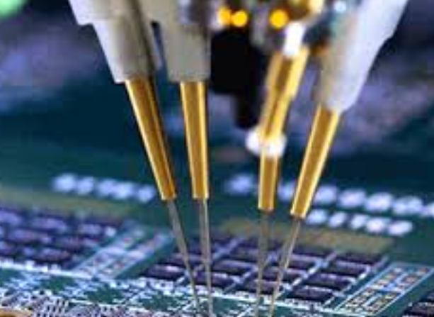
Another advanced technique is In-Circuit Testing (ICT), which involves the use of a bed-of-nails fixture to make electrical contact with various test points on the PCB.
ICT allows for the comprehensive testing of individual components and their interconnections, verifying parameters such as resistance, capacitance, and signal integrity. This method is highly effective for detecting manufacturing defects like open circuits, short circuits, and incorrect component values. Moreover, ICT can be automated, providing rapid and repeatable testing for high-volume production.
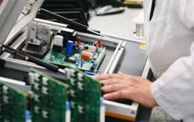
Functional testing is also a critical aspect of PCB quality assurance.
Unlike AOI and ICT, which focus on individual components and connections, functional testing evaluates the PCB as a whole, ensuring that it performs its intended functions under real-world conditions. This type of testing often involves simulating the operating environment and applying various input signals to verify the PCB’s response. Functional testing can identify issues that may not be apparent durtability (DFT) principles are increasingly being integrated into the PCB design process.
DFT involves incorporating features into the PCB layout that facilitate easier and more effective testing.
Examples include adding test points, designing for better accessibility of critical components, and ensuring that the PCB can be easily interfaced with testing equipment. By considering testability during the design phase, manufacturers can reduce the time and cost associated with testing and improve the overall quality of the final product.
Furthermore, advancements in data analytics and machine learning are enhancing PCB testing and quality assurance.
By analyzing large volumes of test data, manufacturers can identify patterns and trends that may indicate underlying issues in the production process. Machine learning algorithms can predict potential defects and optimize testing procedures, leading to more efficient and accurate quality assurance.
In conclusion, advanced techniques for PCB testing and quality assurance are essential for ensuring the reliability and performance of electronic devices. Automated Optical Inspection, X-ray inspection, In-Circuit Testing, functional testing, Design for Testability, and data analytics all play crucial roles in identifying defects and verifying the functionality of assembled PCBs. As technology continues to evolve, these techniques will undoubtedly become even more sophisticated, further enhancing the quality and reliability of electronic products.
Common Challenges In PCB Assembly And How To Overcome Them
Printed Circuit Board (PCB) assembly and testing are critical stages in the electronics manufacturing process, yet they are fraught with numerous challenges that can impact the quality and functionality of the final product.
One of the most common issues encountered during PCB assembly is soldering defects.
These defects, which include solder bridges, cold joints, and insufficient solder, can lead to short circuits, intermittent connections, and ultimately, device failure. To mitigate these problems, it is essential to employ precise soldering techniques and utilize automated soldering equipment that ensures consistent application. Additionally, implementing thorough inspection protocols, such as Automated Optical Inspection (AOI) and X-ray inspection, can help identify and rectify soldering defects early in the assembly process.
Another significant challenge in PCB assembly is component placement accuracy.
With the increasing miniaturization of electronic components, even the slightest misalignment can result in malfunctioning circuits. To address this issue, manufacturers often rely on advanced pick-and-place machines that offer high precision and speed. These machines are equipped with vision systems that accurately position components on the PCB. Furthermore, regular calibration and maintenance of these machines are crucial to maintaining their accuracy over time.
Thermal management is also a critical concern in PCB assembly.
Excessive heat during soldering can damage sensitive components, while inadequate heat dissipation can lead to overheating and reduced lifespan of the device. To overcome this challenge, it is important to use appropriate soldering profiles that match the thermal characteristics of the components and the PCB material. Additionally, incorporating thermal vias, heat sinks, and proper PCB layout design can enhance heat dissipation and ensure reliable operation of the device.
Component availability and supply chain issues pose another challenge in PCB assembly.
The global electronics industry often faces shortages of critical components, leading to production delays and increased costs. To mitigate this risk, manufacturers should establish strong relationships with multiple suppliers and maintain a buffer stock of essential components. Additionally, designing PCBs with alternative components in mind can provide flexibility in case of supply chain disruptions.
Testing is an integral part of the PCB assembly process, yet it presents its own set of challenges.
Ensuring comprehensive testing without damaging the PCB or its components requires a delicate balance. Functional testing, in-circuit testing (ICT), and boundary scan testing are commonly used methods to verify the performance and integrity of assembled PCBs. However, designing effective test fixtures and developing robust test programs can be complex and time-consuming. To streamline this process, manufacturers can leverage automated test equipment (ATE) and software tools that facilitate efficient test development and execution.
Moreover, maintaining high quality and reliability in PCB assembly necessitates adherence to industry standards and best practices.
Standards such as IPC-A-610 and IPC-J-STD-001 provide guidelines for acceptable workmanship and soldering quality. Regular training and certification of assembly personnel ensure that they are well-versed in these standards and can consistently produce high-quality PCBs.
In conclusion, while PCB assembly and testing present numerous challenges, adopting advanced technologies, implementing rigorous inspection and testing protocols, and adhering to industry standards can significantly enhance the quality and reliability of the final product. By addressing issues such as soldering defects, component placement accuracy, thermal management, supply chain disruptions, and testing complexities, manufacturers can overcome these challenges and deliver robust electronic devices that meet the demands of today’s market.
The Role Of Automated Optical Inspection In PCB Manufacturing
Automated Optical Inspection (AOI) has become an indispensable component in the realm of Printed Circuit Board (PCB) manufacturing, playing a pivotal role in ensuring the quality and reliability of electronic assemblies. As the complexity and miniaturization of PCBs continue to advance, the necessity for precise and efficient inspection methods has grown exponentially. AOI systems, leveraging high-resolution cameras and sophisticated algorithms, provide a non-contact method to scrutinize PCBs for defects, thereby enhancing the overall manufacturing process.
Initially, the integration of AOI into PCB manufacturing was driven by the need to detect surface defects such as solder bridges, missing components, and misalignments.
Traditional inspection methods, which relied heavily on manual visual inspection, were not only time-consuming but also prone to human error. The advent of AOI revolutionized this aspect by offering a faster, more accurate, and repeatable solution. By capturing detailed images of the PCB and comparing them against a predefined set of standards, AOI systems can identify discrepancies with remarkable precision.
Moreover, the role of AOI extends beyond mere defect detection.
It also serves as a critical tool for process optimization. By analyzing the data collected during inspection, manufacturers can identify patterns and trends that may indicate underlying issues in the production process. For instance, recurring defects in a specific area of the PCB might suggest a problem with the solder paste application or component placement. Addressing these issues proactively can lead to significant improvements in yield and overall product quality.
In addition to enhancing defect detection and process optimization, AOI contributes to the traceability and documentation of PCB manufacturing. Each inspected board is logged with detailed information about its inspection results, which can be invaluable for quality control and regulatory compliance. This traceability ensures that any issues can be traced back to their source, facilitating root cause analysis and corrective actions. Furthermore, the documentation provided by AOI systems can be used to demonstrate compliance with industry standards and customer requirements, thereby bolstering the manufacturer’s reputation for quality and reliability.
The implementation of AOI in PCB manufacturing is not without its challenges.
One of the primary concerns is the initial cost of the equipment and the need for skilled personnel to operate and maintain the systems. However, the long-term benefits, including reduced defect rates, improved process control, and enhanced traceability, often outweigh these initial investments. Additionally, advancements in AOI technology continue to drive down costs and improve ease of use, making it more accessible to a broader range of manufacturers.
As the electronics industry continues to evolve, the importance of AOI in PCB manufacturing is likely to grow even further
Emerging technologies such as artificial intelligence and machine learning are poised to enhance the capabilities of AOI systems, enabling even more sophisticated defect detection and process optimization. By leveraging these advancements, manufacturers can stay ahead of the curve, ensuring that their products meet the highest standards of quality and reliability.
In conclusion, Automated Optical Inspection plays a crucial role in PCB manufacturing by providing a fast, accurate, and reliable method for defect detection and process optimization. Its contributions to traceability and documentation further underscore its value in ensuring quality and compliance. Despite the initial challenges associated with its implementation, the long-term benefits make AOI an essential tool for modern PCB manufacturers. As technology continues to advance, the role of AOI is set to become even more integral to the success of the electronics industry