Pcb assembly automation
Importance Of Solder Paste Inspection In Pcb assembly automation
In the realm of printed circuit board (PCB) assembly, the importance of solder paste inspection (SPI) cannot be overstated. As the initial step in the surface mount technology (SMT) process, solder paste application sets the foundation for the entire assembly.
Consequently, ensuring the accuracy and quality of this application is paramount. Solder paste, a mixture of powdered solder and flux, is applied to the PCB through a stencil, adhering to the pads where components will be placed. Any deviation in the amount or placement of solder paste can lead to significant issues down the line, such as poor solder joints, bridging, or open circuits.
Transitioning to the inspection phase, SPI serves as a critical quality control measure.
By employing advanced optical and laser-based systems, SPI machines meticulously examine the solder paste deposits. These systems measure various parameters, including volume, height, area, and alignment of the paste. Detecting discrepancies at this stage allows for immediate corrective actions, thereby preventing defects from propagating through subsequent assembly processes. This early intervention is crucial, as it is far more cost-effective to address issues at the solder paste stage than to rework or scrap a fully assembled PCB.
Moreover, the role of SPI extends beyond mere defect detection. It also provides valuable data for process optimization.
By analyzing trends and patterns in solder paste application, manufacturers can identify underlying issues in the stencil design, printing process, or material properties. This data-driven approach enables continuous improvement, enhancing the overall yield and reliability of PCB assemblies. Furthermore, integrating SPI data with other inspection and testing results creates a comprehensive feedback loop, fostering a more robust and efficient manufacturing process.
In addition to its technical benefits, SPI also plays a significant role in meeting industry standards and customer expectations.
High-reliability sectors, such as aerospace, medical devices, and automotive, demand stringent quality control measures to ensure the safety and performance of their products. Implementing SPI as part of the PCB assembly process demonstrates a commitment to quality and compliance with industry standards, such as IPC-A-610 and ISO 9001. This not only enhances the manufacturer’s reputation but also builds trust with customers and end-users.
Transitioning to the broader implications, the importance of SPI is further underscored by the increasing complexity and miniaturization of electronic components.
As PCBs become more densely populated with smaller and more intricate components, the margin for error in solder paste application diminishes. In such scenarios, even minor deviations can have significant repercussions on the functionality and reliability of the final product. Therefore, investing in advanced SPI technology becomes indispensable for manufacturers aiming to stay competitive in the rapidly evolving electronics industry.
In conclusion, solder paste inspection is a vital component of the PCB assembly process, offering numerous benefits that extend from defect prevention to process optimization and compliance with industry standards. By ensuring the accuracy and quality of solder paste application, SPI not only enhances the reliability and performance of PCB assemblies but also contributes to the overall efficiency and competitiveness of the manufacturing process. As the electronics industry continues to advance, the role of SPI will undoubtedly become even more critical, underscoring its importance in achieving high-quality, reliable electronic products.

Techniques For Effective PCB Testing And Troubleshooting
Printed Circuit Board (PCB) assembly and testing are critical stages in the electronics manufacturing process, ensuring that the final product functions as intended. Effective PCB testing and troubleshooting techniques are essential to identify and rectify any issues that may arise during assembly. These techniques not only enhance the reliability of the product but also reduce the time and cost associated with post-production repairs.
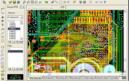
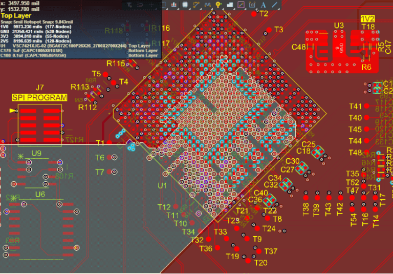
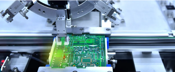
One of the primary techniques for effective PCB testing is the use of Automated Optical Inspection (AOI).
AOI systems employ high-resolution cameras to capture images of the PCB and compare them against a predefined template. This method is particularly useful for detecting surface defects such as solder bridges, missing components, and misalignments. By automating the inspection process, AOI significantly reduces human error and speeds up the detection of faults, thereby improving overall production efficiency.
In addition to AOI, In-Circuit Testing (ICT) is another vital technique.
ICT involves the use of a bed-of-nails tester to make electrical contact with various points on the PCB. This method allows for the verification of component values, circuit continuity, and signal integrity. ICT is highly effective in identifying issues such as open circuits, short circuits, and incorrect component placements. Moreover, it provides quantitative data that can be used for further analysis and troubleshooting.
Functional testing is also an indispensable technique in PCB testing.
Unlike AOI and ICT, which focus on individual components and connections, functional testing evaluates the PCB as a whole. This method involves simulating the operating conditions of the final product and verifying that the PCB performs its intended functions. Functional testing is particularly useful for identifying issues that may not be apparent during earlier stages of testing, such as software-related problems or interactions between different components.
Transitioning from testing to troubleshooting, it is essential to have a systematic approach to identify and rectify issues.
One effective method is the use of a fault tree analysis (FTA). FTA involves creating a visual representation of potential faults and their causes, allowing engineers to systematically investigate and eliminate possible issues. This method is particularly useful for complex PCBs with multiple layers and components, as it helps to narrow down the root cause of the problem.
Another valuable troubleshooting technique is the use of thermal imaging.
Thermal cameras can detect hotspots on the PCB, which may indicate issues such as excessive current flow, short circuits, or overheating components. By identifying these hotspots, engineers can quickly pinpoint the location of the problem and take corrective action. Thermal imaging is especially useful for identifying issues that may not be visible through traditional inspection methods.
Furthermore, signal integrity analysis is crucial for troubleshooting high-speed PCBs.
This technique involves the use of oscilloscopes and network analyzers to measure signal quality and identify issues such as reflections, crosstalk, and impedance mismatches. By analyzing the signal integrity, engineers can make necessary adjustments to the PCB design or layout to ensure optimal performance.
In conclusion, effective PCB testing and troubleshooting techniques are essential for ensuring the reliability and functionality of electronic products. Techniques such as Automated Optical Inspection, In-Circuit Testing, and functional testing play a crucial role in identifying and rectifying issues during the assembly process. Additionally, systematic troubleshooting methods such as fault tree analysis, thermal imaging, and signal integrity analysis are invaluable tools for engineers. By employing these techniques, manufacturers can enhance product quality, reduce production costs, and ensure customer satisfaction.
Role Of Automated Optical Inspection In PCB Manufacturing
Automated Optical Inspection (AOI) plays a pivotal role in the realm of Printed Circuit Board (PCB) manufacturing, serving as a critical checkpoint in ensuring the quality and reliability of electronic assemblies. As the complexity and density of PCBs continue to escalate, the necessity for precise and efficient inspection methods becomes increasingly paramount. AOI systems, leveraging advanced imaging technologies and sophisticated algorithms, have emerged as indispensable tools in the quest for defect-free PCB production.
Initially, it is essential to understand the fundamental principles of AOI.
These systems utilize high-resolution cameras to capture detailed images of the PCB. Subsequently, these images are analyzed using pattern recognition software to detect any deviations from the intended design. This process encompasses the inspection of various aspects, including component placement, solder joint integrity, and the presence of foreign materials. By identifying defects at an early stage, AOI systems significantly mitigate the risk of faulty products reaching the end-user, thereby enhancing overall product reliability.
Transitioning to the benefits of AOI, one of the most notable advantages is its ability to perform inspections at a rapid pace.
Traditional manual inspection methods are not only time-consuming but also prone to human error. In contrast, AOI systems can inspect thousands of components per hour with remarkable accuracy. This efficiency is particularly beneficial in high-volume production environments, where time is of the essence. Moreover, the consistency and repeatability of AOI systems ensure that every PCB is subjected to the same rigorous inspection criteria, thereby maintaining uniform quality standards.
Furthermore, AOI systems contribute to cost savings in PCB manufacturing.
By detecting defects early in the production process, manufacturers can avoid the expenses associated with rework and scrap. Early detection also prevents defective products from progressing to subsequent stages of assembly, where the cost of rectification would be significantly higher. Additionally, AOI systems can be integrated seamlessly into existing production lines, minimizing disruption and maximizing return on investment.
Another critical aspect to consider is the role of AOI in enhancing traceability and process control.
Modern AOI systems are equipped with data logging capabilities, enabling manufacturers to track inspection results and identify trends over time. This data-driven approach facilitates continuous improvement by pinpointing recurring issues and enabling targeted corrective actions. Consequently, manufacturers can refine their processes, reduce defect rates, and achieve higher levels of operational efficiency.
Moreover, the versatility of AOI systems cannot be overstated.
These systems are adaptable to a wide range of PCB designs and can be configured to inspect various types of components, from surface-mounted devices to through-hole components. This flexibility ensures that AOI systems remain relevant and effective, even as PCB designs evolve and new technologies emerge.
In conclusion, Automated Optical Inspection is an integral component of modern PCB manufacturing, offering a multitude of benefits that enhance product quality, operational efficiency, and cost-effectiveness. By leveraging advanced imaging and analysis technologies, AOI systems provide a reliable and efficient means of detecting defects, ensuring that only the highest quality products reach the market. As the demand for increasingly complex and miniaturized electronic devices continues to grow, the role of AOI in PCB manufacturing will undoubtedly become even more critical, cementing its status as a cornerstone of quality assurance in the electronics industry.
Best Practices For Surface Mount Technology (SMT) Assembly
Surface Mount Technology (SMT) assembly is a critical process in the production of modern electronic devices, requiring meticulous attention to detail and adherence to best practices to ensure high-quality outcomes. One of the fundamental aspects of SMT assembly is the proper handling and storage of components. Components should be stored in a controlled environment to prevent exposure to moisture, which can lead to defects such as solder joint failures. Utilizing moisture barrier bags and desiccants, along with regular monitoring of humidity levels, can significantly mitigate these risks.
Another essential practice is the precise application of solder paste.
The solder paste must be applied uniformly and in the correct amount to ensure reliable connections between components and the printed circuit board (PCB). This is typically achieved through stencil printing, where a stencil with apertures corresponding to the PCB pads is used to deposit the solder paste. Ensuring the stencil is clean and properly aligned is crucial for achieving consistent results. Additionally, the type of solder paste used should be selected based on the specific requirements of the assembly, such as the type of components and the operating environment of the final product.
Component placement is another critical step in SMT assembly.
Automated pick-and-place machines are commonly used to place components onto the PCB with high precision. It is important to regularly calibrate these machines to maintain accuracy and prevent misalignment. Furthermore, the components should be inspected for any defects or damage before placement, as this can affect the overall reliability of the assembly. Implementing automated optical inspection (AOI) systems can help identify and rectify placement issues early in the process.
Once the components are placed, the next step is reflow soldering, where the solder paste is melted to form a permanent bond between the components and the PCB.
The reflow process must be carefully controlled to ensure proper solder joint formation. This involves setting the correct temperature profile, which includes preheating, soaking, reflow, and cooling stages. Each stage must be precisely controlled to prevent issues such as solder bridging, tombstoning, or insufficient wetting. Regularly monitoring and adjusting the reflow oven settings can help maintain optimal soldering conditions.
Post-reflow inspection is another best practice that cannot be overlooked.
This involves examining the solder joints and components to ensure they meet the required quality standards. Techniques such as X-ray inspection can be used to detect hidden defects, such as voids or insufficient solder coverage, that are not visible through traditional optical inspection methods. Implementing a robust inspection process helps identify defects early, reducing the likelihood of failures in the final product.
Finally, functional testing of the assembled PCB is essential to verify that it operates as intended.
This can include in-circuit testing (ICT) to check for electrical continuity and functionality, as well as functional testing to simulate the actual operating conditions of the device. Ensuring that the testing procedures are thorough and comprehensive helps identify any issues that may have been missed during the assembly process.
In conclusion, adhering to best practices in SMT assembly is vital for producing high-quality electronic devices. Proper handling and storage of components, precise solder paste application, accurate component placement, controlled reflow soldering, thorough post-reflow inspection, and comprehensive functional testing are all critical steps that contribute to the overall reliability and performance of the final product. By following these best practices, manufacturers can achieve consistent and reliable results in their SMT assembly processes.