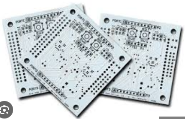
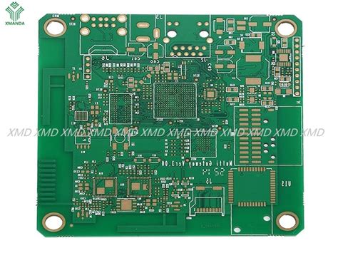
PCB Assembly Drawing Methods to Boost Manufacturing Accuracy
Key Takeaways
Effective PCB assembly design relies on precision across three core elements: component placement, tolerance specifications, and design validation. Optimizing these factors minimizes errors in PCBA workflows, ensuring seamless transitions from prototyping to mass production. For instance, strategically positioning high-density components reduces signal interference, while clearly defined mechanical and electrical tolerances prevent mismatches during solder paste application.
A critical yet often overlooked practice is validating designs through automated rule checks (ARCs) and 3D modeling, which identify collisions or alignment issues before manufacturing. Below is a comparison of traditional versus optimized approaches:
| Aspect | Traditional Approach | Optimized Approach |
|---|---|---|
| Component Placement | Manual spacing adjustments | Algorithm-driven cluster analysis |
| Tolerance Specs | ±10% general guidelines | Layer-specific ±5% thresholds |
| Design Validation | Post-production testing | Pre-fabrication simulation |
| Error Rate | 12-18% rework | <5% post-assembly fixes |
By integrating advanced drafting software with real-time collaboration features, teams can synchronize updates across mechanical and electrical domains, reducing ambiguities in PCB assembly drawings. This alignment ensures manufacturing partners receive unambiguous instructions, cutting delays caused by misinterpretations.
PCB Assembly Drawing Precision Tips
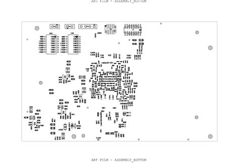
Achieving manufacturing accuracy in PCB assembly begins with meticulously detailed drawings that eliminate ambiguity. A well-structured PCBA design specifies exact component coordinates and orientation markers, ensuring automated placement systems operate with micron-level precision. Critical dimensions should include tolerance specs (±0.1mm for high-density boards) to account for thermal expansion and material variations during production.
Tip: Use CAD tools to overlay component footprints with manufacturer datasheets, reducing mismatches between design intent and physical parts.
For error reduction, prioritize reference designators and polarity indicators in silkscreen layers, especially for surface-mount devices (SMDs). Clear annotations for test points and fiducial markers streamline optical alignment in pick-and-place machines. Cross-referencing bill of materials (BOM) data with assembly layers minimizes discrepancies—a common source of rework.
Integrating design validation protocols early in workflows ensures compatibility with fabrication capabilities. For instance, annular ring checks and pad-to-trace spacing analyses prevent solder bridging or lifted pads. Additionally, layer-specific color coding in drawings aids visual verification, while 3D renderings expose potential mechanical conflicts before prototyping.
Finally, maintain version control across all PCBA documentation to synchronize design revisions with manufacturing updates. This practice avoids costly mismatches between prototype iterations and mass-production batches, preserving both accuracy and timeline integrity.
Component Placement Error Reduction
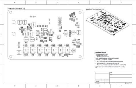
Critical to successful PCB assembly, precise component placement directly impacts functionality and manufacturability. Modern PCBA workflows leverage computer-aided design (CAD) tools to automate placement, reducing human error while ensuring alignment with design intent. Engineers optimize layouts by defining clearance rules and footprint accuracy in assembly drawings, which guide pick-and-place machines to position components within micron-level tolerances.
A key strategy involves implementing reference designators and polarity indicators to eliminate ambiguity during assembly. For example, silkscreen markings paired with 3D models in drawings help operators verify orientations for ICs, connectors, and polarized capacitors. Additionally, thermal management zones and mechanical stress points should be annotated to avoid placing sensitive components near high-heat areas or board edges.
To further minimize errors, designers must validate PCB assembly drawings through design-for-manufacturing (DFM) checks. These reviews identify conflicts such as overlapping pads or mismatched land patterns, which could cause misalignment during soldering. Integrating automated optical inspection (AOI) criteria into drawings ensures post-assembly quality control aligns with geometric specifications. By standardizing these practices, PCBA teams achieve consistent placement accuracy, reducing rework and accelerating time-to-market.
Tolerance Specs in PCB Manufacturing
Effective PCB assembly relies on meticulously defined tolerance specifications that govern dimensional and positional accuracy across the manufacturing process. By establishing ±0.1mm tolerances for features like soldermask clearances and plated through-hole diameters, designers ensure components align precisely during PCBA stages. These specifications act as guardrails against cumulative errors, particularly critical in high-density designs where even minor deviations can compromise solder joint integrity or electrical connectivity.
Modern tolerance analysis tools enable designers to simulate worst-case scenarios, identifying potential conflicts between component footprints and fabrication capabilities. For instance, specifying IPC-6012 Class 3 tolerances for military-grade boards requires tighter controls on annular ring widths compared to commercial applications. Material selection also influences tolerance requirements, as substrates with higher coefficients of thermal expansion demand allowances for dimensional shifts during reflow soldering.
Proper documentation of geometric dimensioning and tolerancing (GD&T) in PCB assembly drawings eliminates ambiguity between design intent and manufacturing execution. This precision reduces rework rates by up to 27% in multilayer PCBA projects, according to industry benchmarks. Manufacturers increasingly rely on statistical process control to maintain tolerances across batch productions, ensuring consistent quality without over-constraining fabrication parameters.
Design Validation in PCB Workflows
Effective PCB assembly relies on rigorous design validation to bridge the gap between theoretical layouts and manufacturable outcomes. This process involves systematic checks to ensure PCBA designs adhere to electrical, mechanical, and thermal requirements before reaching production. Advanced tools like design rule checks (DRC) and 3D modeling software identify conflicts in component spacing, solder mask alignment, or via placement, which could lead to assembly defects.
Integrating simulation-based validation further optimizes workflows by predicting thermal stress or signal integrity issues under real-world conditions. For instance, validating high-density interconnect (HDI) designs ensures PCB assembly teams can execute complex routing without compromising reliability. Collaboration between designers and PCBA manufacturers during this phase also clarifies tolerance thresholds and material compatibility, reducing ambiguities in fabrication specs.
Automated validation protocols, such as IPC-2581 or Gerber-X3 file reviews, standardize error detection across layers, minimizing rework risks. By embedding validation checkpoints early in the design cycle, teams preemptively address mismatches between CAD models and production realities, ensuring seamless transitions from prototyping to mass manufacturing. This proactive approach not only accelerates timelines but also fortifies the precision demanded by modern electronics manufacturing.
Accurate Drafting Enhances Workflow
Precision in PCB assembly documentation directly impacts manufacturing efficiency by eliminating ambiguities that cause delays or rework. Standardized drafting practices ensure fabrication teams interpret component placements, layer stackups, and critical dimensions consistently. For instance, clearly defining PCBA-specific requirements—such as solder mask clearances or thermal relief patterns—reduces misinterpretations during solder paste application or reflow processes.
A well-structured assembly drawing integrates tolerance specifications for hole sizes, pad alignments, and interlayer spacing, which are vital for maintaining signal integrity in high-frequency designs. By establishing unambiguous callouts for surface finishes or component orientation, manufacturers avoid costly deviations during automated pick-and-place operations. Tools like geometric dimensioning and tolerancing (GD&T) further enhance clarity, enabling precise communication between design and production teams.
Moreover, iterative design validation workflows—cross-referencing assembly drawings with 3D models—identify mechanical conflicts early, such as connector interference or inadequate heatsink clearances. This alignment between digital prototypes and physical layouts minimizes post-production adjustments, ensuring seamless transitions from prototyping to mass-scale PCB assembly. As a result, accurate drafting not only accelerates timelines but also reinforces quality control across electronics manufacturing ecosystems.
Minimize Electronics Assembly Errors
Effective PCB assembly processes rely on meticulous attention to component positioning and design documentation. A primary strategy involves optimizing component placement to prevent overlaps, misalignments, or spacing violations that trigger soldering defects. By adhering to PCBA design rules—such as maintaining adequate clearance between high-density components—manufacturers reduce risks of short circuits or tombstoning during reflow soldering.
Equally critical is the enforcement of tolerance specifications in fabrication files. Clear annotations for hole sizes, pad dimensions, and layer alignment ensure that automated assembly equipment operates within precise parameters. For instance, specifying ±0.1mm tolerances for surface-mount device (SMD) footprints minimizes placement inaccuracies caused by machine calibration drift.
Design validation tools further enhance error reduction by simulating assembly outcomes before production. Software-driven checks identify conflicts between bill of materials (BOM) data and physical layouts, flagging discrepancies like mismatched component footprints. Integrating design for manufacturability (DFM) principles at this stage helps eliminate rework cycles, as engineers can adjust pad geometries or thermal relief patterns proactively.
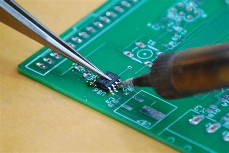
Lastly, standardized annotation practices in PCB assembly drawings—such as polarity markers, pin-1 indicators, and fiducial alignments—streamline technician workflows. Consistent use of reference designators and assembly notes ensures that even complex PCBA configurations are interpreted correctly, reducing human error during manual inspections or part placement.
Advanced PCB Drawing Techniques
Modern PCB assembly processes demand precision-driven drafting methodologies to ensure seamless translation from design to production. Implementing 3D modeling tools enables engineers to visualize component placement in relation to mechanical enclosures, identifying spatial conflicts before PCBA fabrication begins. By integrating design-for-manufacturability (DFM) guidelines, critical parameters such as pad geometries, solder mask clearances, and via placements are optimized to match automated assembly workflows.
Leveraging layer stack-up configurations with explicit dielectric specifications ensures signal integrity while accommodating thermal management needs. For high-density designs, parametric dimensioning tools standardize hole diameters, trace widths, and pitch measurements, reducing tolerance stack-up risks during PCB assembly. Additionally, material annotations for substrates and finishes (e.g., FR-4, Rogers, or ENIG coatings) guide manufacturers in selecting compatible soldering profiles.
To further minimize errors, advanced workflows incorporate testability features like embedded fiducial markers or boundary scan points directly into assembly drawings. Pairing these with revision-controlled documentation ensures all stakeholders reference the latest specifications, bridging gaps between design iterations and production batches. Such techniques not only accelerate PCBA validation but also establish repeatable frameworks for complex electronics manufacturing.
Conclusion
Ultimately, the precision of PCB assembly drawings directly determines the success of PCBA manufacturing processes. By focusing on critical factors like tolerance specifications, component placement accuracy, and rigorous design validation, manufacturers can significantly reduce defects and rework. These practices ensure that every layer of the PCB assembly aligns with functional and mechanical requirements, enabling seamless integration into final products.
Adopting advanced drafting tools and standardized workflows further enhances consistency across batches, particularly for high-volume PCBA production. Emphasizing clear documentation—from solder mask definitions to drill hole alignments—eliminates ambiguities that often lead to costly delays. As electronics grow more complex, the role of meticulous PCB assembly drawings becomes indispensable in bridging design intent with manufacturing execution. By prioritizing precision at every drafting stage, teams can achieve faster time-to-market while maintaining the reliability demanded by modern applications.
Frequently Asked Questions
How do assembly drawings improve accuracy in PCB manufacturing?
PCB assembly drawings provide precise visual and technical guidelines, ensuring correct component placement and orientation. By detailing solder joints, layer stackups, and mechanical dimensions, they minimize misinterpretation during PCBA production.
What design elements are critical for reducing assembly errors?
Clear tolerance specifications for hole sizes, pad spacing, and alignment are essential. Additionally, annotations for polarity markings and reference designators help technicians avoid misalignment or reversed parts during PCB assembly.
Why is design validation crucial before finalizing drawings?
Validation checks identify conflicts between schematics and physical layouts, such as overlapping traces or insufficient clearance. This step ensures manufacturing accuracy by resolving issues before PCBA fabrication begins.
Can automated tools replace manual reviews of assembly drawings?
While tools like DFM (Design for Manufacturability) software detect common errors, manual reviews remain vital for contextual analysis. Combining both methods optimizes error detection in PCB assembly workflows.
How does standardized documentation streamline electronics manufacturing?
Uniform drawing formats improve communication between designers and manufacturers, reducing delays from clarification requests. Consistent tolerance specs and layer notations also enhance repeatability across PCBA batches.
Ready to Optimize Your PCB Assembly Process?
For expert guidance on creating precision-driven PCB assembly drawings, please click here to explore tailored solutions for your manufacturing needs.