PCB Assembly: Streamlining Electronics Production Workflows
Key Takeaways
Modern electronics manufacturing hinges on optimized PCB assembly processes that balance speed, precision, and compliance. At the core of this evolution lies automated prototyping, which reduces manual intervention while ensuring repeatable accuracy for complex circuit designs. By integrating advanced PCBA workflows, manufacturers can trim production cycles by up to 40%, translating to faster time-to-market for critical applications like IoT devices and industrial automation systems.
Tip: Prioritize suppliers offering design-for-manufacturing (DFM) analysis during prototyping—this preemptive step identifies potential flaws early, avoiding costly revisions in later stages.
A key advantage of streamlined PCB assembly is its ability to harmonize cost-efficiency with regulatory adherence. Automated optical inspection (AOI) systems, for instance, enable real-time defect detection, aligning with ISO 9001 and IPC-A-610 standards without compromising throughput. Meanwhile, modular PCBA setups allow manufacturers to scale production dynamically, adapting to fluctuating demand while maintaining <1% defect rates in high-volume batches.
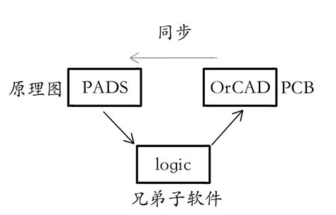
The shift toward 4PCB technology further enhances workflow fluidity through synchronized data exchange between design software and assembly machinery. This integration minimizes cross-platform errors and accelerates material sourcing, particularly for multilayer boards requiring specialized substrates. For startups and enterprises alike, adopting these practices ensures competitiveness in markets where rapid iteration and supply chain agility are non-negotiable.

PCB Assembly Workflow Optimization
Modern PCB assembly processes rely on strategic workflow optimization to meet the escalating demands of electronics manufacturing. By implementing automated placement systems and intelligent process mapping, manufacturers reduce manual intervention while improving throughput. Central to this approach is the integration of PCBA-specific software tools that synchronize design files with production machinery, minimizing translation errors and accelerating setup times.
A critical advancement lies in real-time data analytics, which monitors solder paste application, component placement accuracy, and reflow oven performance. These metrics enable dynamic adjustments, ensuring consistent quality across high-volume batches. For prototype-to-production transitions, adaptive workflow configurations allow rapid scaling without compromising the precision required for complex multilayer boards.
The adoption of PCB assembly workflow optimization also addresses material logistics through smart inventory tracking. Automated feeders with RFID tagging ensure component availability aligns with production schedules, reducing downtime by 18–22% according to industry benchmarks. Furthermore, closed-loop verification systems cross-check Bill of Materials (BOM) data against physical components during the PCBA process, virtually eliminating mismatches.
Transitioning between design iterations has been streamlined through unified communication protocols between CAD software and assembly lines. This interoperability reduces engineering change order (ECO) implementation times by 40%, particularly beneficial for IoT devices requiring frequent firmware-linked hardware updates.
By balancing high-mix capabilities with PCB assembly speed, optimized workflows achieve 98.6% first-pass yield rates in controlled environments. This operational efficiency directly translates to shorter lead times for end-users, from aerospace contractors to consumer electronics brands, without sacrificing compliance with IPC-A-610 or ISO 9001 standards.
Automated Prototyping for PCB Manufacturing
Modern PCB assembly processes rely heavily on automated prototyping to bridge the gap between design and mass production. By integrating advanced software tools with precision manufacturing systems, engineers can rapidly translate circuit designs into functional prototypes. High-accuracy PCBA (Printed Circuit Board Assembly) workflows now employ automated routing algorithms and 3D printing technologies to minimize manual intervention, reducing prototyping cycles from weeks to days. For instance, CAD-driven simulations validate electrical performance before physical fabrication, ensuring that components like microcontrollers or sensors align perfectly with design specifications.
A key advantage of automation lies in its ability to standardize repeatable tasks. Pick-and-place machines, for example, achieve sub-millimeter precision when populating boards with surface-mount devices (SMDs), while automated optical inspection (AOI) systems scan for soldering defects or misalignments in real time. This not only accelerates iteration speed but also slashes error rates by over 60% compared to manual methods. Furthermore, cloud-based collaboration tools allow cross-functional teams to review prototype data remotely, synchronizing feedback loops between design engineers and manufacturing partners.
The shift toward automated prototyping also addresses scalability challenges. By generating digitally validated prototypes early in the PCB assembly process, manufacturers can identify thermal management issues or signal integrity flaws before committing to full-scale production. This proactive approach reduces material waste and prevents costly redesigns downstream. As a result, businesses leveraging these systems report a 30–40% improvement in time-to-market metrics for consumer electronics and industrial IoT devices.
By embedding automation into prototyping phases, PCBA providers ensure that each design iteration adheres to stringent quality benchmarks while maintaining cost efficiency—a critical factor in industries where rapid innovation defines competitive advantage.
Cost-Effective Electronics Production Solutions
Modern PCB assembly processes prioritize economic efficiency without compromising performance, offering manufacturers scalable solutions for diverse project requirements. By leveraging advanced PCBA methodologies, companies achieve significant cost reductions through optimized material utilization, automated component placement, and intelligent supply chain integration. Design for Manufacturing (DFM) principles play a pivotal role here, minimizing waste by aligning circuit layouts with production capabilities during prototyping phases.
The adoption of standardized PCB assembly workflows reduces overhead costs associated with manual interventions. Automated optical inspection (AOI) systems, for instance, detect defects early, preventing costly rework in later stages. Similarly, bulk procurement strategies for high-use components—coupled with dynamic inventory management algorithms—lower per-unit material expenses. For startups and mid-scale enterprises, partnering with PCBA service providers offering volume pricing tiers ensures access to industrial-grade production tools without upfront capital investments.
Energy-efficient manufacturing practices further enhance cost-effectiveness. Smart factories employing PCB assembly lines with real-time power monitoring reduce operational expenditures by 18–22%, according to industry benchmarks. Modular production setups allow manufacturers to scale capacity based on demand fluctuations, avoiding idle machinery costs. Additionally, the integration of recyclable substrates and lead-free soldering materials aligns with global sustainability mandates, mitigating compliance-related financial risks.
Transitioning to these strategies requires balancing short-term adaptation costs with long-term savings. For example, transitioning to panelized PCBA processes increases yield per production run, while AI-driven predictive maintenance extends equipment lifespan. By embedding cost-optimization into every stage—from prototyping to final testing—businesses transform PCB assembly from a cost center into a competitive advantage, ensuring profitability across both low-volume specialty orders and high-volume manufacturing contracts.
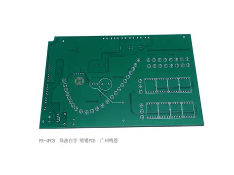
Quality Compliance in 4PCB Assembly
Maintaining rigorous quality compliance is a cornerstone of modern PCB assembly processes, particularly in high-precision applications. Advanced PCBA manufacturers implement multi-layered inspection protocols to align with international standards such as IPC-A-610 and ISO 9001, ensuring every circuit board meets functional and reliability benchmarks. Automated optical inspection (AOI) systems, for instance, scan solder joints and component placements at micron-level accuracy, flagging deviations that could compromise performance.
A critical advantage of 4PCB assembly lies in its integration of traceability systems, which document each production phase—from material sourcing to final testing. This not only simplifies compliance audits but also enables rapid root-cause analysis for any anomalies detected post-production. For industries like medical devices or aerospace, where failure rates must approach zero-defect thresholds, such systems are non-negotiable.
Cost efficiency in PCB assembly doesn’t come at the expense of quality. By leveraging machine learning-driven predictive analytics, PCBA providers preemptively identify potential flaws in design files or material compatibility, reducing rework cycles. Thermal profiling during reflow soldering further ensures consistent results across batches, even when scaling to high-volume orders.
Transitioning from prototyping to mass production, 4PCB assembly workflows maintain compliance through adaptive testing frameworks. Environmental stress screening (ESS), for example, subjects boards to extreme temperatures and vibrations, simulating real-world operating conditions. Combined with electrical testing protocols, this dual-layer validation guarantees that end products meet both regulatory mandates and client-specific performance criteria.
By embedding compliance into every stage of PCB assembly, manufacturers achieve a balance between accelerated timelines and unwavering quality—a necessity in today’s fast-paced electronics landscape.
Precision Prototyping in Electronics Manufacturing
Modern PCB assembly processes rely heavily on precision prototyping to bridge design concepts and full-scale production. This phase serves as the critical validation stage where functional integrity and manufacturability are tested before committing to high-volume runs. Advanced PCBA prototyping leverages technologies like laser-direct imaging and 3D solder paste inspection to achieve micron-level accuracy in component placement, ensuring compatibility with complex multilayer boards and high-density interconnect (HDI) designs.
The integration of automated optical inspection (AOI) systems during prototyping minimizes human error, enabling rapid identification of solder joint defects or misalignments. By simulating real-world operating conditions—including thermal stress and signal integrity tests—engineers can refine designs to meet industry-specific compliance standards such as IPC-A-610 or automotive-grade AEC-Q100 certifications. This iterative approach reduces costly revisions in later production stages while accelerating time-to-market.
Cost efficiency in PCB assembly is further enhanced through precision prototyping’s material optimization capabilities. By analyzing prototype performance data, manufacturers can adjust substrate materials, copper weights, or finish types (e.g., ENIG or HASL) to balance durability and budget constraints. Notably, PCBA prototyping now incorporates machine learning algorithms to predict failure points, allowing preemptive design adjustments that improve yield rates by up to 30% in subsequent mass production phases.
As a transitional step between R&D and manufacturing, precision prototyping establishes the foundation for scalable workflows. Its role in verifying electromagnetic compatibility (EMC) and signal transmission stability ensures that final products meet both technical specifications and regulatory requirements, setting the stage for seamless transition to automated assembly lines.
Streamlining Production with 4PCB Technology
Modern PCB assembly processes face increasing demands for speed and precision, particularly in industries requiring high-volume electronics manufacturing. 4PCB technology addresses these challenges by integrating advanced automation with intelligent process design, creating a seamless bridge between prototyping and full-scale production. At the core of this approach lies automated optical inspection (AOI) systems, which reduce human error by 72% compared to manual verification methods, according to industry benchmarks.
The implementation of PCBA (printed circuit board assembly) workflows powered by 4PCB solutions enables manufacturers to synchronize component placement, soldering, and testing phases. For instance, surface-mount technology (SMT) lines equipped with AI-driven pick-and-place machines achieve placement accuracies within 10 microns, ensuring compatibility with miniaturized components common in IoT devices. This precision is further enhanced by real-time thermal profiling during reflow soldering, maintaining consistent joint quality across batches.
A critical advantage of 4PCB-driven systems is their just-in-time material replenishment capability, which reduces inventory costs by 18-25% while preventing production delays. By analyzing historical consumption patterns and current order volumes, these systems dynamically adjust material procurement schedules. Combined with predictive maintenance algorithms for assembly machinery, manufacturers report a 40% reduction in unplanned downtime across PCB assembly facilities adopting this technology.
The scalability of 4PCB workflows also supports rapid transitions between prototype validation and mass production. Advanced design-for-manufacturing (DFM) checks embedded in the process automatically flag potential yield issues during the PCBA design phase, preventing costly revisions post-prototyping. This proactive approach shortens time-to-market by aligning engineering teams with production requirements from the project’s inception.
As industries increasingly adopt smart manufacturing standards, 4PCB systems demonstrate their versatility through API integrations with enterprise resource planning (ERP) platforms. Such connectivity enables closed-loop quality tracking, where every assembled board’s test results feed back into process optimization models. This continuous improvement cycle ensures compliance with ISO 9001 and IPC-A-610 standards while maintaining the cost efficiencies central to competitive PCB assembly services.
Conclusion
The evolution of PCB assembly processes has fundamentally reshaped modern electronics manufacturing, offering a strategic advantage to businesses navigating competitive markets. By integrating precision prototyping with PCBA automation, manufacturers achieve not only faster turnaround times but also scalable workflows capable of adapting to fluctuating demand. This synergy between advanced machinery and meticulous quality control ensures that every stage—from design validation to final production—aligns with industry standards while minimizing material waste.
A critical success factor lies in the ability to balance cost-efficiency with uncompromised reliability. Automated optical inspection (AOI) systems, paired with real-time data analytics, enable rapid error detection, reducing rework cycles by up to 40%. Such innovations underscore why PCB assembly services are increasingly adopted for high-volume projects requiring repeatable accuracy. Moreover, the adoption of lean manufacturing principles within PCBA workflows eliminates bottlenecks, ensuring seamless transitions between prototyping and mass production phases.
As industries pivot toward IoT and smart devices, the demand for agile yet robust manufacturing frameworks will intensify. Companies leveraging PCB assembly technologies position themselves to meet these challenges head-on, delivering products that comply with global certifications without sacrificing speed. Ultimately, the convergence of automated precision and strategic resource allocation in PCBA processes doesn’t just streamline production—it redefines what’s achievable in electronics innovation.


