PCB Board Selection Guide: Key Factors to Consider
Printed Circuit Boards (PCBs) are the backbone of modern electronics, serving as the foundation for nearly all electronic devices. Choosing the right PCB is crucial for ensuring performance, reliability, and cost-effectiveness in your project. This comprehensive guide will walk you through the key factors to consider when selecting a PCB, including material, layer count, thickness, surface finish, and more.
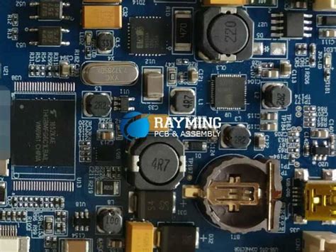
1. Understanding PCB Basics
Before diving into selection criteria, it’s essential to understand the basic types of PCBs:
- Single-Layer PCBs: The simplest type, with conductive material on one side.
- Double-Layer PCBs: Conductive layers on both sides, allowing for more complex circuits.
- Multi-Layer PCBs: Three or more conductive layers, used in high-density applications.
- Flexible PCBs: Made from flexible materials like polyimide, ideal for wearable and compact devices.
- Rigid-Flex PCBs: Combine rigid and flexible sections for complex designs.
- High-Frequency PCBs: Designed for RF and microwave applications.
Each type serves different purposes, so identifying your project’s requirements is the first step.
2. PCB Material Selection
The choice of PCB material affects electrical performance, thermal management, and durability. Common materials include:
A. FR-4 (Flame Retardant 4)
- Pros: Cost-effective, good mechanical strength, widely available.
- Cons: Limited high-frequency performance.
- Best for: Consumer electronics, industrial controls.
B. High-Tg FR-4 (High Glass Transition Temperature)
- Pros: Better thermal resistance than standard FR-4.
- Cons: Slightly more expensive.
- Best for: High-power and high-temperature applications.
C. Polyimide
- Pros: Excellent flexibility, high thermal stability.
- Cons: More expensive than FR-4.
- Best for: Aerospace, medical devices, flexible PCBs.
D. PTFE (Teflon)
- Pros: Superior high-frequency performance, low dielectric loss.
- Cons: Expensive, harder to manufacture.
- Best for: RF, microwave, and high-speed digital circuits.
E. Metal-Core (MCPCB)
- Pros: Excellent heat dissipation.
- Cons: Higher cost, limited layer count.
- Best for: LED lighting, power electronics.
3. PCB Layer Count
The number of layers determines the complexity and functionality of the PCB:
- 1-2 Layers: Simple circuits, low-cost projects.
- 4-6 Layers: Common in consumer electronics (smartphones, IoT devices).
- 8+ Layers: High-speed digital systems (servers, telecom equipment).
Considerations:
- More layers allow for better signal integrity but increase cost.
- High-speed designs may require controlled impedance layers.
4. Copper Thickness
Copper thickness impacts current-carrying capacity and thermal performance. Common options:
- 0.5 oz/ft² (17.5 µm): Low-power applications.
- 1 oz/ft² (35 µm): Standard for most PCBs.
- 2 oz/ft² (70 µm) and above: High-current applications (power supplies, motor controllers).
Tip: Thicker copper improves heat dissipation but may require wider traces to avoid etching issues.
5. PCB Thickness
Standard PCB thickness ranges from 0.2 mm to 3.2 mm, with 1.6 mm being the most common.
Selection Factors:
- Mechanical Strength: Thicker boards are more durable.
- Component Compatibility: Some connectors require specific thicknesses.
- Flexibility: Thin PCBs are used in compact and flexible designs.
6. Surface Finish Options
The surface finish protects copper from oxidation and ensures solderability. Common choices:
| Finish Type | Pros | Cons | Best For |
|---|---|---|---|
| HASL (Hot Air Solder Leveling) | Low cost, widely available | Uneven surface, not ideal for fine-pitch components | Consumer electronics |
| ENIG (Electroless Nickel Immersion Gold) | Flat surface, good for fine-pitch components | More expensive than HASL | High-reliability applications |
| OSP (Organic Solderability Preservative) | Cost-effective, eco-friendly | Limited shelf life | Low-cost, short-life products |
| Immersion Silver | Good solderability, moderate cost | Tarnishes over time | RF and high-frequency circuits |
| ENEPIG (Electroless Nickel Electroless Palladium Immersion Gold) | Excellent for wire bonding, high reliability | Very expensive | Aerospace, medical devices |
7. Trace Width and Spacing
Proper trace width and spacing ensure signal integrity and prevent short circuits.
- Standard Traces: 0.15 mm to 0.3 mm (6-12 mils).
- High-Current Traces: Wider traces (e.g., 1 mm or more) for power lines.
- High-Speed Signals: Controlled impedance traces with precise spacing.
Design Tip: Use a PCB trace width calculator to determine optimal dimensions based on current and temperature rise.
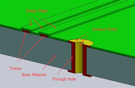
8. Via Types
Vias connect different layers in a PCB. Common types:
- Through-Hole Vias: Standard, goes through all layers.
- Blind Vias: Connects outer layer to inner layer (not fully through).
- Buried Vias: Connects inner layers only (not visible outside).
- Microvias: Small vias (≤ 0.15 mm) for HDI (High-Density Interconnect) PCBs.
Selection Criteria:
- Cost: Blind/buried vias increase manufacturing complexity.
- Space Constraints: Microvias save space in compact designs.
9. Thermal Management
Overheating can damage components. Consider:
- Thermal Vias: Help dissipate heat from hot components.
- Heatsinks: Attached to high-power components.
- Copper Pour: Large copper areas improve heat spreading.
For High-Power Designs: Use metal-core PCBs (MCPCBs) or thermal substrates.
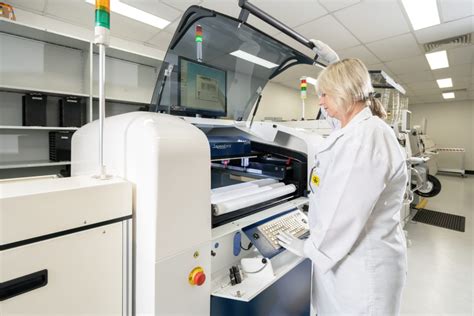
10. Manufacturing and Cost Considerations
- Prototype vs. Mass Production: Small batches may cost more per unit.
- Tolerances: Tighter tolerances increase cost.
- Lead Time: Standard PCBs take 5-10 days, while complex ones may take longer.
Cost-Saving Tips:
- Use standard materials (FR-4) where possible.
- Avoid unnecessary layers and advanced finishes.
- Panelize designs to reduce per-unit costs.
11. Reliability and Testing
Ensure your PCB meets quality standards:
- IPC-A-600: Defects acceptability for PCBs.
- IPC-6012: Performance and qualification specifications.
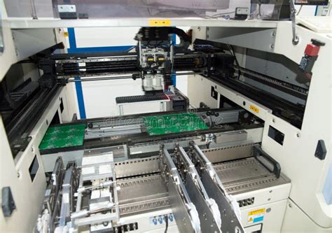
- Testing Methods:
- Visual Inspection: Checks for obvious defects.
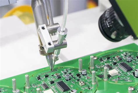
- Automated Optical Inspection (AOI): Detects soldering and assembly issues.
- Electrical Testing: Verifies connectivity (Flying Probe, Bed of Nails).
12. Environmental Considerations
- RoHS Compliance: Lead-free manufacturing for environmental safety.
- High-Temperature Resistance: Needed for automotive/aerospace applications.
- Moisture Protection: Conformal coating for humid environments.
Conclusion
Selecting the right PCB involves balancing performance, cost, and manufacturability. Key takeaways:
- Choose the right material (FR-4, polyimide, PTFE, etc.) based on electrical and thermal needs.
- Optimize layer count—more layers allow complexity but increase cost.
- Select appropriate surface finish (ENIG, HASL, OSP) for solderability and reliability.
- Ensure proper trace width, spacing, and vias for signal integrity.
- Consider thermal management for high-power designs.
- Verify manufacturing tolerances and testing standards for reliability.
By carefully evaluating these factors, you can select the best PCB for your project, ensuring optimal performance and longevity. Whether you’re designing a simple IoT device or a high-speed computing system, the right PCB choice is critical to success.