PCB CAD Design: Exploring 3D Design and Top View Perspectives
Introduction to PCB CAD Design
Printed Circuit Board (PCB) Computer-Aided Design (CAD) has revolutionized the electronics industry by providing powerful tools for designing complex circuit layouts with precision and efficiency. In modern electronics development, PCB CAD software has become indispensable, enabling engineers to create everything from simple single-layer boards to sophisticated multi-layer designs with high-density interconnects.
The evolution of PCB design tools has progressed from simple 2D layout programs to advanced 3D modeling environments that can simulate the entire electronic assembly. This technological advancement has significantly reduced development time, improved design accuracy, and enhanced the overall quality of electronic products.
Among the various visualization options available in PCB CAD software, the top view perspective remains one of the most fundamental and frequently used views in the design process. However, the integration of 3D design capabilities has added a new dimension to PCB development, allowing designers to visualize and verify their boards in ways that were previously impossible.
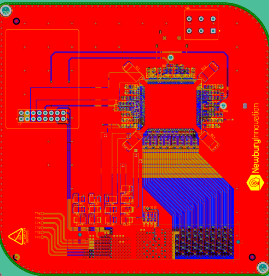
The Importance of Top View in PCB Design
The top view perspective in PCB CAD software provides the primary working interface for most layout tasks. This two-dimensional representation shows the board from above, displaying all components, traces, and features as they would appear looking directly down on the assembled PCB.
Key Elements Visible in Top View
- Component Placement: The top view clearly shows the position and orientation of all surface-mounted and through-hole components on the component side of the board.
- Trace Routing: All copper traces connecting components are visible, showing their paths, widths, and connections to pads and vias.
- Copper Pour Areas: Large areas of copper used for power planes or ground connections are easily identifiable in top view.
- Board Outline: The physical shape and dimensions of the PCB are clearly defined.
- Reference Designators: Component labels and identifiers are typically displayed in this view for easy reference.
Advantages of Top View Design
The top view perspective offers several benefits in the PCB design process:
- Simplified Layout: Working in 2D allows designers to focus on the logical connections between components without the complexity of 3D space.
- Efficient Routing: Trace routing algorithms often work most effectively in the 2D top view environment.
- Clear Documentation: Manufacturing files and assembly drawings are typically generated from top view perspectives.
- Faster Processing: 2D operations generally require less computational power than 3D rendering, enabling faster design iterations.
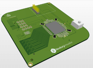
Transition to 3D PCB Design
While the top view remains essential, modern PCB CAD systems have incorporated robust 3D design capabilities that provide significant advantages throughout the design process.
Benefits of 3D PCB Design
- Mechanical Integration: 3D visualization allows designers to check how the PCB fits within its enclosure and interacts with other mechanical components.
- Component Clearance Verification: Potential collisions between tall components or with the enclosure can be identified early in the design process.
- Thermal Analysis: 3D models enable more accurate thermal simulations by considering the spatial relationships between heat-generating components.
- Manufacturing Validation: Potential assembly issues can be spotted before production begins.
- Realistic Prototyping: Stakeholders can visualize the final product more accurately through 3D renderings.
3D Component Libraries
Modern PCB CAD systems maintain extensive 3D component libraries that include accurate mechanical models of common electronic parts. These libraries allow designers to:
- Import standard component models in various formats (STEP, IGES, etc.)
- Create custom 3D models for proprietary components
- Associate 3D models with schematic symbols and footprint patterns
- Adjust component heights and orientations for accurate representation
Integrating Top View and 3D Perspectives
The most effective PCB design workflow combines both top view and 3D perspectives, using each where most appropriate.
Workflow Integration
- Initial Layout: Begin with traditional top view for schematic capture and initial component placement.
- Basic Routing: Perform fundamental trace routing in 2D for efficiency.
- 3D Verification: Switch to 3D view to check mechanical constraints and clearances.
- Iterative Refinement: Alternate between views to optimize both electrical and mechanical aspects.
- Final Validation: Use 3D for comprehensive design rule checking (DRC) that includes spatial constraints.
Synchronized Viewing Modes
Advanced PCB CAD systems offer synchronized viewing capabilities:
- Cross-Probing: Selecting a component in one view highlights it in all other views
- Simultaneous Display: Split-screen or picture-in-picture options to see multiple perspectives at once
- View-Specific Tools: Specialized tools optimized for each viewing perspective
Design Considerations in Top View vs. 3D
Different aspects of PCB design receive varying emphasis depending on the viewing perspective:
Top View Focus Areas
- Signal Integrity: Trace lengths, impedance matching, and signal path optimization
- Power Distribution: Power plane segmentation and decoupling capacitor placement
- Manufacturing Constraints: Minimum trace widths, spacing rules, and solder mask requirements
- Testability: Access points for testing and debugging
3D View Focus Areas
- Mechanical Fit: Board dimensions relative to enclosure and mounting points
- Component Height: Clearance for tall components and heat sinks
- Connector Alignment: Proper orientation of external interfaces
- Assembly Sequence: Accessibility for automated or manual assembly processes
Advanced Visualization Techniques
Modern PCB CAD systems employ sophisticated visualization techniques to enhance both top view and 3D design:
Top View Enhancements
- Layer Stack Visualization: Color-coded representations of different layers with adjustable transparency
- Net Highlighting: Emphasizing complete electrical connections across the board
- Design Rule Markers: Visual indicators of potential violations
- Signal Flow Animation: Dynamic display of signal paths
3D Visualization Features
- Realistic Rendering: Photorealistic materials and lighting effects
- Section Views: Cutting planes to inspect internal board features
- Exploded Views: Showing component relationships before assembly
- Animation: Simulating insertion/removal or flexing of flexible PCBs
Manufacturing Output from Different Perspectives
Both top view and 3D data play important roles in manufacturing preparation:
Top View Manufacturing Outputs
- Gerber Files: Industry-standard 2D representations of each layer
- Drill Files: NC drill data for hole locations and sizes
- Assembly Drawings: Component placement documentation
- Silkscreen Artwork: Legend printing information
3D Manufacturing Outputs
- STEP Files: 3D models for mechanical CAD integration
- Assembly Guides: 3D animations or illustrations for production staff
- Tooling Verification: Checking fixture compatibility
- Automated Optical Inspection (AOI): Reference models for quality control
Future Trends in PCB Visualization
The future of PCB CAD design visualization includes several promising developments:
- Augmented Reality (AR) Integration: Overlaying PCB designs onto physical spaces for prototyping and maintenance
- Virtual Reality (VR) Design Environments: Immersive 3D spaces for collaborative PCB development
- AI-Assisted Visualization: Intelligent systems that automatically highlight potential issues
- Real-Time Multi-User Collaboration: Cloud-based simultaneous editing with synchronized views
- Enhanced Simulation Integration: Combining visualization with electrical, thermal, and mechanical simulations

Best Practices for Using Top View and 3D in PCB Design
To maximize the benefits of both perspectives, designers should:
- Establish View-Switching Routines: Regularly alternate between views to catch different types of issues
- Maintain Consistent Libraries: Ensure 2D footprints and 3D models are properly associated and updated
- Customize Display Settings: Optimize visibility of critical features in each view
- Leverage Cross-Highlighting: Use selection tools that work across multiple views
- Document in Multiple Formats: Create both 2D and 3D documentation for different stakeholders
Conclusion
The combination of traditional top view and modern 3D perspectives in PCB CAD design offers a comprehensive approach to electronic product development. While the top view remains essential for detailed layout and routing tasks, 3D visualization provides critical insights into mechanical integration and physical constraints.
As PCB technology continues to advance with higher densities, more complex layer stacks, and tighter integration with mechanical components, the ability to seamlessly work across both 2D and 3D environments becomes increasingly important. Designers who master both perspectives and understand when to apply each will produce higher quality boards with fewer revisions and faster time-to-market.
The future of PCB CAD design promises even more sophisticated visualization tools that will further blur the lines between electrical and mechanical design, enabling a truly holistic approach to electronic product development. By embracing both the precision of top view design and the contextual awareness of 3D modeling, engineers can create innovative solutions that meet the growing demands of modern electronics.